

DAC5662IPFB
Product Overview
Category: Digital-to-Analog Converter (DAC)
Use: The DAC5662IPFB is a high-performance digital-to-analog converter designed for various applications that require precise and accurate analog output signals. It is commonly used in audio systems, telecommunications equipment, industrial automation, and test and measurement instruments.
Characteristics: - High resolution: The DAC5662IPFB offers a resolution of up to 16 bits, ensuring fine-grained control over the analog output. - Fast conversion speed: With a maximum sampling rate of 500 Mega Samples Per Second (MSPS), it can quickly convert digital input signals into analog output signals. - Low power consumption: The DAC5662IPFB is designed to operate efficiently with low power consumption, making it suitable for battery-powered devices. - Wide voltage range: It supports a wide supply voltage range, typically from 1.8V to 3.6V, allowing flexibility in different system designs.
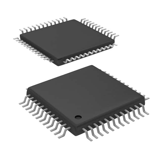
Package: The DAC5662IPFB is available in a small form factor package, such as a lead-free, 48-pin TQFP (Thin Quad Flat Package). This package ensures easy integration into various circuit boards and provides reliable electrical connections.
Essence: The DAC5662IPFB is a key component in digital signal processing systems, enabling the conversion of digital data into analog signals with high precision and fidelity.
Packaging/Quantity: The DAC5662IPFB is typically sold in reels or tubes, containing a specified quantity of units per package. The exact packaging and quantity may vary depending on the supplier.
Specifications
- Resolution: Up to 16 bits
- Sampling Rate: Up to 500 MSPS
- Supply Voltage Range: 1.8V to 3.6V
- Power Consumption: Low power design
- Package Type: 48-pin TQFP
Detailed Pin Configuration
The DAC5662IPFB has a total of 48 pins, each serving a specific function. The pin configuration is as follows:
- VREFP: Positive reference voltage input
- VREFN: Negative reference voltage input
- AGND: Analog ground
- AVDD: Analog power supply
- DVDD: Digital power supply
- DGND: Digital ground
- CLK: Clock input
- DATA: Digital data input
- SYNC: Synchronization input
- RESET: Reset input
- OUTA: Analog output A
- OUTB: Analog output B 13-48: Reserved for other functions
Please refer to the datasheet or product documentation for a complete pin configuration diagram.
Functional Features
- High-resolution digital-to-analog conversion
- Fast and accurate signal processing
- Low power consumption for energy-efficient operation
- Wide voltage range for flexible system integration
- Reliable electrical connections with the small form factor package
Advantages and Disadvantages
Advantages: - High resolution allows for precise analog output - Fast conversion speed enables real-time applications - Low power consumption extends battery life - Wide voltage range provides flexibility in system design - Small form factor package ensures easy integration
Disadvantages: - May require additional external components for optimal performance - Higher cost compared to lower-end DACs - Limited availability from certain suppliers
Working Principles
The DAC5662IPFB operates based on the principle of converting digital input signals into corresponding analog output signals. It utilizes advanced digital signal processing techniques to accurately reconstruct the analog waveform from the digital data.
The digital input signals are received through the DATA pin and synchronized using the CLK and SYNC inputs. The internal circuitry then processes the digital data and generates the analog output signals on the OUTA and OUTB pins. The resolution and sampling rate determine the accuracy and speed of the conversion process.
Detailed Application Field Plans
The DAC5662IPFB finds applications in various fields, including:
- Audio Systems: Used in high-fidelity audio equipment to convert digital audio signals into analog signals for amplification and playback.
- Telecommunications Equipment: Enables precise signal generation and modulation in communication systems, such as wireless base stations and satellite communication devices.
- Industrial Automation: Provides accurate control signals for industrial automation processes, such as motor control and robotics.
- Test and Measurement Instruments: Used in test equipment to generate precise analog signals for testing and calibration purposes.
Detailed and Complete Alternative Models
- DAC5682ZIRGC: Similar high-performance DAC with enhanced features
- DAC5642IPFB: Lower-resolution DAC with similar characteristics
- DAC5672IPFB: Higher-resolution DAC with comparable specifications
- DAC5622IPFB: Lower-cost DAC with reduced performance
These alternative models offer different trade-offs in terms of resolution, cost, and specific features. It is recommended to consult the respective datas
Lista 10 Vanliga frågor och svar relaterade till tillämpningen av DAC5662IPFB i tekniska lösningar
Sure! Here are 10 common questions and answers related to the application of DAC5662IPFB in technical solutions:
Q: What is DAC5662IPFB? A: DAC5662IPFB is a digital-to-analog converter (DAC) integrated circuit that converts digital signals into analog signals.
Q: What is the purpose of using DAC5662IPFB in technical solutions? A: DAC5662IPFB is commonly used to convert digital data into analog signals for applications such as audio processing, instrumentation, and communication systems.
Q: What is the resolution of DAC5662IPFB? A: DAC5662IPFB has a resolution of 16 bits, which means it can represent analog signals with high precision.
Q: What is the maximum sampling rate supported by DAC5662IPFB? A: DAC5662IPFB supports a maximum sampling rate of 500 MegaSamples per second (MSPS).
Q: How does DAC5662IPFB connect to a microcontroller or FPGA? A: DAC5662IPFB typically connects to a microcontroller or FPGA through a serial interface such as SPI (Serial Peripheral Interface) or I2C (Inter-Integrated Circuit).
Q: Can DAC5662IPFB operate on a single power supply voltage? A: Yes, DAC5662IPFB can operate on a single power supply voltage ranging from 1.8V to 3.6V.
Q: Does DAC5662IPFB support differential output? A: Yes, DAC5662IPFB supports differential output, which provides better noise immunity and signal integrity.
Q: What is the output voltage range of DAC5662IPFB? A: The output voltage range of DAC5662IPFB is typically between 0V and the reference voltage (Vref) supplied to the IC.
Q: Can DAC5662IPFB be used in high-speed communication systems? A: Yes, DAC5662IPFB is suitable for high-speed communication systems such as wireless base stations and radar applications.
Q: Are there any evaluation boards or development kits available for DAC5662IPFB? A: Yes, Texas Instruments provides evaluation boards and development kits for DAC5662IPFB, which can help in prototyping and testing applications.
Please note that the answers provided here are general and may vary depending on the specific implementation and requirements of your technical solution.