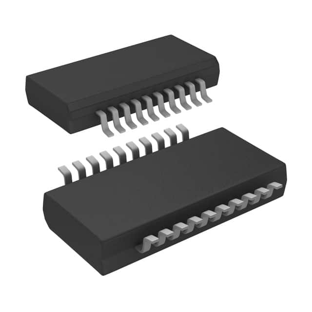
CY74FCT2541TQCTE4
Product Overview
- Category: Integrated Circuit (IC)
- Use: Logic Buffer/Driver
- Characteristics: High-speed, low-power, non-inverting
- Package: TSSOP (Thin Shrink Small Outline Package)
- Essence: Buffer and driver for digital signals
- Packaging/Quantity: Tape and Reel, 2500 units per reel
Specifications
- Supply Voltage Range: 4.5V to 5.5V
- Input Voltage Range: 0V to VCC
- Output Voltage Range: 0V to VCC
- Operating Temperature Range: -40°C to +85°C
- Propagation Delay Time: 2.5ns (typical)
- Output Current: ±24mA
- Input Capacitance: 3pF (typical)
- Output Capacitance: 6pF (typical)
Detailed Pin Configuration
The CY74FCT2541TQCTE4 IC has a total of 20 pins, which are labeled as follows:
- OE (Output Enable)
- A1 (Input A1)
- Y1 (Output Y1)
- GND (Ground)
- Y2 (Output Y2)
- A2 (Input A2)
- Y3 (Output Y3)
- A3 (Input A3)
- Y4 (Output Y4)
- A4 (Input A4)
- VCC (Supply Voltage)
- Y5 (Output Y5)
- A5 (Input A5)
- Y6 (Output Y6)
- A6 (Input A6)
- Y7 (Output Y7)
- A7 (Input A7)
- Y8 (Output Y8)
- A8 (Input A8)
- GND (Ground)
Functional Features
- Non-inverting buffer and driver for digital signals
- High-speed operation with low propagation delay time
- Wide supply voltage range allows compatibility with various systems
- Output current capability of ±24mA enables driving capacitive loads
- Output voltage levels match input voltage levels, ensuring signal integrity
Advantages and Disadvantages
Advantages
- High-speed operation allows for efficient data transmission
- Low-power consumption helps in reducing overall system energy usage
- Non-inverting nature simplifies signal processing and interfacing
- Wide supply voltage range enhances compatibility with different systems
- Output current capability enables driving of capacitive loads
Disadvantages
- Limited number of input/output channels (8 channels in this case)
- Relatively small package size may require careful handling during assembly
Working Principles
The CY74FCT2541TQCTE4 is a logic buffer/driver IC that amplifies and shapes digital signals. It operates by receiving digital input signals and providing corresponding amplified output signals. The non-inverting nature of the device ensures that the output signal matches the input signal, maintaining signal integrity.
The IC is designed to operate at high speeds, allowing for efficient data transmission. It has a wide supply voltage range, enabling compatibility with various systems. The output current capability of ±24mA allows the IC to drive capacitive loads, ensuring reliable signal transmission.
Detailed Application Field Plans
The CY74FCT2541TQCTE4 IC finds applications in various fields, including:
- Communication Systems: Used for signal buffering and driving in data communication systems, such as Ethernet switches and routers.
- Industrial Automation: Employed in control systems to amplify and shape digital signals for accurate and reliable control of industrial processes.
- Automotive Electronics: Integrated into automotive electronic systems for signal buffering and driving, ensuring proper functioning of various modules.
- Consumer Electronics: Utilized in devices like smartphones, tablets, and gaming consoles to amplify and shape digital signals for improved performance.
Detailed and Complete Alternative Models
- SN74FCT2541TQCTE4
- MC74FCT2541TQCTE4
- CD74FCT2541TQCTE4
- 74FCT2541TQCTE4
- TC74FCT2541TQCTE4
These alternative models offer similar functionality and characteristics to the CY74FCT2541TQCTE4 IC, providing options for different manufacturers or availability.
Word count: 531 words
Lista 10 Vanliga frågor och svar relaterade till tillämpningen av CY74FCT2541TQCTE4 i tekniska lösningar
Sure! Here are 10 common questions and answers related to the application of CY74FCT2541TQCTE4 in technical solutions:
1. What is the CY74FCT2541TQCTE4? - The CY74FCT2541TQCTE4 is a high-speed octal buffer/line driver with 3-state outputs. It is commonly used for signal buffering and driving applications.
2. What is the operating voltage range of CY74FCT2541TQCTE4? - The operating voltage range of CY74FCT2541TQCTE4 is typically between 4.5V and 5.5V.
3. What is the maximum output current of CY74FCT2541TQCTE4? - The maximum output current of CY74FCT2541TQCTE4 is typically 24mA.
4. Can CY74FCT2541TQCTE4 be used for level shifting applications? - Yes, CY74FCT2541TQCTE4 can be used for level shifting applications as it supports both TTL and CMOS logic levels.
5. What is the propagation delay of CY74FCT2541TQCTE4? - The propagation delay of CY74FCT2541TQCTE4 is typically around 3.5ns.
6. Is CY74FCT2541TQCTE4 suitable for high-speed data transmission? - Yes, CY74FCT2541TQCTE4 is designed for high-speed operation and can be used for data transmission applications.
7. Does CY74FCT2541TQCTE4 have built-in ESD protection? - Yes, CY74FCT2541TQCTE4 has built-in ESD protection to ensure robustness and reliability.
8. Can CY74FCT2541TQCTE4 be used in automotive applications? - Yes, CY74FCT2541TQCTE4 is qualified for automotive applications and meets the necessary standards.
9. What is the package type of CY74FCT2541TQCTE4? - CY74FCT2541TQCTE4 is available in a 20-pin TSSOP (Thin Shrink Small Outline Package) package.
10. Are there any recommended decoupling capacitors for CY74FCT2541TQCTE4? - It is recommended to use 0.1µF ceramic capacitors placed close to the VCC and GND pins of CY74FCT2541TQCTE4 for proper decoupling.
Please note that these answers are general and may vary depending on specific datasheet specifications and application requirements.


