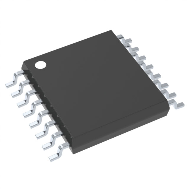
CDCVF25084PWR
Overview
Category: Integrated Circuit
Use: Clock Driver
Characteristics: High-speed, low-jitter, low-power
Package: TSSOP
Essence: Clock distribution and buffering
Packaging/Quantity: Tape and Reel, 2500 pieces per reel
Specifications and Parameters
- Supply Voltage: 2.3V to 3.6V
- Operating Temperature Range: -40°C to +85°C
- Output Frequency Range: DC to 200MHz
- Number of Outputs: 10
- Output Type: LVCMOS/LVTTL
- Input Type: LVCMOS/LVTTL
- Input Frequency Range: DC to 200MHz
- Input Level: CMOS/TTL compatible
- Output Skew: 100ps (maximum)
- Propagation Delay: 1.5ns (maximum)
Pin Configuration
The CDCVF25084PWR has a total of 20 pins. The pin configuration is as follows:
- VDD
- GND
- OUT0
- OUT1
- OUT2
- OUT3
- OUT4
- OUT5
- OUT6
- OUT7
- OUT8
- OUT9
- OE#
- CLK
- SEL0
- SEL1
- SEL2
- SEL3
- SEL4
- NC
Functional Characteristics
- Clock input can be selected from five different sources using the SEL0-SEL4 pins.
- Output enable (OE#) pin allows for disabling all outputs simultaneously.
- Low output skew ensures accurate clock distribution.
- Supports both LVCMOS and LVTTL input/output levels.
- Wide operating voltage range allows for flexibility in various applications.
- Low power consumption for energy-efficient designs.
Advantages and Disadvantages
Advantages: - High-speed clock distribution with low jitter. - Wide operating temperature range. - Multiple output options for versatile applications. - Low power consumption. - Compact TSSOP package for space-constrained designs.
Disadvantages: - Limited number of outputs (10). - Not suitable for high-frequency applications above 200MHz. - Requires external clock source.
Applicable Range of Products
The CDCVF25084PWR is commonly used in electronic devices that require precise clock distribution, such as:
- Communication equipment
- Networking devices
- Data storage systems
- Industrial automation
- Test and measurement instruments
Working Principles
The CDCVF25084PWR is a clock driver integrated circuit that receives an input clock signal and distributes it to multiple output channels. The device allows the selection of the clock source from five different inputs using the SEL0-SEL4 pins. The selected clock is then buffered and distributed to the ten output channels. The output enable (OE#) pin can be used to disable all outputs simultaneously.
Detailed Application Field Plans
Communication Equipment: The CDCVF25084PWR can be used to distribute clock signals in routers, switches, and other network communication devices, ensuring synchronized data transmission.
Data Storage Systems: In storage area networks and RAID systems, the CDCVF25084PWR can provide accurate clock distribution, improving data access and reliability.
Industrial Automation: Clock synchronization is crucial in industrial automation applications. The CDCVF25084PWR ensures precise timing for PLCs, motor control systems, and robotic devices.
Test and Measurement Instruments: Oscilloscopes, logic analyzers, and other test equipment require accurate clock signals. The CDCVF25084PWR enables reliable clock distribution in these instruments.
Automotive Electronics: In-car infotainment systems, navigation devices, and advanced driver-assistance systems (ADAS) rely on precise clock synchronization. The CDCVF25084PWR can be used to distribute clocks in automotive electronics.
Detailed Alternative Models
CDCVF25084APWR: Similar to CDCVF25084PWR but with an extended operating temperature range (-55°C to +125°C).
CDCVF25084BQDRQ1: Automotive-grade version of CDCVF25084PWR with enhanced ESD protection and AEC-Q100 qualification.
CDCVF25084EVM: Evaluation module for the CDCVF25084PWR, providing a platform for testing and prototyping.
CDCVF25084RGZT: RoHS-compliant version of CDCVF25084PWR with lead-free package.
CDCVF25084IPW: Industrial-grade version of CDCVF25084PWR with extended temperature range (-40°C to +105°C) and higher reliability.
5 Common Technical Questions and Answers
- Q: What is the maximum output frequency supported by the


