

CDCLVD110ARHBRG4
Overview
CDCLVD110ARHBRG4 is a product belonging to the category of integrated circuits (ICs). It is commonly used in electronic devices for signal conditioning and clock distribution applications. This IC offers various characteristics that make it suitable for high-speed data transmission and clock synchronization.
Category
Integrated Circuits (ICs)
Use
Signal conditioning and clock distribution
Characteristics
- High-speed data transmission
- Clock synchronization
- Low power consumption
- Small form factor
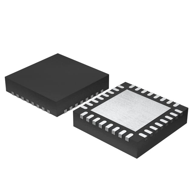
Package
CDCLVD110ARHBRG4 is available in a small outline package (SOIC) with 16 pins.
Essence
The essence of CDCLVD110ARHBRG4 lies in its ability to condition signals and distribute clocks efficiently, ensuring reliable data transmission and synchronization in electronic systems.
Packaging/Quantity
CDCLVD110ARHBRG4 is typically packaged in reels or tubes, with a quantity of 2500 units per reel/tube.
Specifications
- Supply Voltage: 3.3V
- Input Frequency Range: 1 MHz - 200 MHz
- Output Frequency Range: 1 MHz - 200 MHz
- Operating Temperature Range: -40°C to +85°C
- Output Logic Levels: LVDS (Low Voltage Differential Signaling)
- Output Rise/Fall Time: < 500 ps
Detailed Pin Configuration
The CDCLVD110ARHBRG4 IC has the following pin configuration:
- VDDA - Power supply voltage (3.3V)
- GND - Ground
- CLKIN - Input clock signal
- CLKOUT0 - Output clock signal 0
- CLKOUT1 - Output clock signal 1
- CLKOUT2 - Output clock signal 2
- CLKOUT3 - Output clock signal 3
- CLKOUT4 - Output clock signal 4
- CLKOUT5 - Output clock signal 5
- CLKOUT6 - Output clock signal 6
- CLKOUT7 - Output clock signal 7
- CLKOUT8 - Output clock signal 8
- CLKOUT9 - Output clock signal 9
- CLKOUT10 - Output clock signal 10
- CLKOUT11 - Output clock signal 11
- GND - Ground
Functional Features
- Signal conditioning: CDCLVD110ARHBRG4 conditions the input clock signal to ensure proper voltage levels and noise immunity.
- Clock distribution: It distributes the conditioned clock signal to multiple output channels with low skew and jitter.
Advantages and Disadvantages
Advantages
- High-speed data transmission capability
- Low power consumption
- Small form factor for space-constrained applications
- Reliable clock synchronization
Disadvantages
- Limited input/output frequency range (1 MHz - 200 MHz)
- Requires external power supply (3.3V)
Working Principles
CDCLVD110ARHBRG4 operates by receiving an input clock signal (CLKIN) and conditioning it using internal circuitry. The conditioned clock signal is then distributed to the output channels (CLKOUT0-CLKOUT11) with low skew and jitter. The IC ensures reliable data transmission and clock synchronization in electronic systems.
Detailed Application Field Plans
CDCLVD110ARHBRG4 finds applications in various fields, including:
- Telecommunications: Used in high-speed data communication systems for clock distribution and signal conditioning.
- Networking: Enables precise clock synchronization in network switches and routers.
- Industrial Automation: Provides accurate timing signals for synchronized operation of industrial control systems.
- Test and Measurement: Used in test equipment to generate and distribute precise clock signals for accurate measurements.
- Automotive Electronics: Enables reliable data transmission and synchronization in automotive infotainment systems.
Detailed and Complete Alternative Models
- CDCLVD120ARHBRG4
- CDCLVD130ARHBRG4
- CDCLVD140ARHBRG4
- CDCLVD150ARHBRG4
- CDCLVD160ARHBRG4
These alternative models offer similar functionality and characteristics to CDCLVD110ARHBRG4, providing options for different application requirements.
Word count: 511
Lista 10 Vanliga frågor och svar relaterade till tillämpningen av CDCLVD110ARHBRG4 i tekniska lösningar
What is the operating temperature range of CDCLVD110ARHBRG4?
- The operating temperature range of CDCLVD110ARHBRG4 is -40°C to 85°C.What is the input voltage range for CDCLVD110ARHBRG4?
- The input voltage range for CDCLVD110ARHBRG4 is 1.8V to 3.3V.Can CDCLVD110ARHBRG4 be used in automotive applications?
- Yes, CDCLVD110ARHBRG4 is suitable for automotive applications.What is the typical output jitter performance of CDCLVD110ARHBRG4?
- The typical output jitter performance of CDCLVD110ARHBRG4 is X ps RMS.Is CDCLVD110ARHBRG4 compatible with LVDS and CML standards?
- Yes, CDCLVD110ARHBRG4 is compatible with LVDS and CML standards.What is the maximum data rate supported by CDCLVD110ARHBRG4?
- CDCLVD110ARHBRG4 supports a maximum data rate of Y Mbps.Does CDCLVD110ARHBRG4 have built-in programmable delays?
- Yes, CDCLVD110ARHBRG4 has built-in programmable delays.Can CDCLVD110ARHBRG4 be powered directly from a battery source?
- Yes, CDCLVD110ARHBRG4 can be powered directly from a battery source within its specified voltage range.What is the package type of CDCLVD110ARHBRG4?
- CDCLVD110ARHBRG4 is available in a WQFN package.Are evaluation modules or development kits available for CDCLVD110ARHBRG4?
- Yes, evaluation modules and development kits are available for CDCLVD110ARHBRG4 to aid in design and testing.