

CD74AC540M96
Product Overview
- Category: Integrated Circuit (IC)
- Use: Logic Level Shifter
- Characteristics: High-speed, low-power consumption
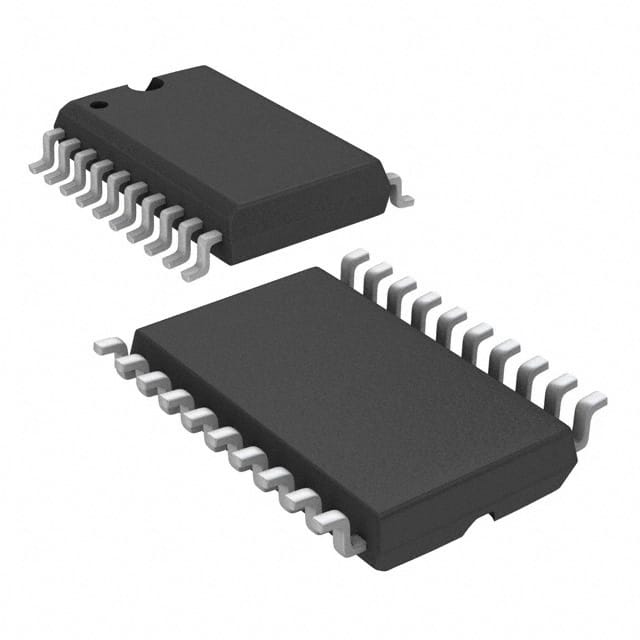
- Package: 20-pin SOIC (Small Outline Integrated Circuit)
- Essence: Logic level shifting between different voltage domains
- Packaging/Quantity: Tape and Reel, 2500 units per reel
Specifications
- Supply Voltage: 2V to 6V
- Logic Family: AC
- Number of Channels: 8
- Input Voltage Levels: TTL/CMOS compatible
- Output Voltage Levels: TTL/CMOS compatible
- Propagation Delay: 5ns typical, 10ns maximum
- Operating Temperature Range: -40°C to +85°C
Detailed Pin Configuration
The CD74AC540M96 has a total of 20 pins. The pin configuration is as follows:
- GND (Ground)
- A1 (Input A1)
- B1 (Input B1)
- Y1 (Output Y1)
- A2 (Input A2)
- B2 (Input B2)
- Y2 (Output Y2)
- A3 (Input A3)
- B3 (Input B3)
- Y3 (Output Y3)
- A4 (Input A4)
- B4 (Input B4)
- Y4 (Output Y4)
- VCC (Positive Power Supply)
- OE (Output Enable)
- Y5 (Output Y5)
- A5 (Input A5)
- B5 (Input B5)
- Y6 (Output Y6)
- GND (Ground)
Functional Features
- Provides bidirectional logic level shifting between different voltage domains
- Supports TTL and CMOS compatible input and output voltage levels
- High-speed operation with low propagation delay
- Low power consumption for efficient energy usage
- Output enable (OE) pin for easy control of the output state
Advantages and Disadvantages
Advantages
- Enables seamless interfacing between devices operating at different voltage levels
- Wide supply voltage range allows compatibility with various systems
- Fast propagation delay ensures quick signal transmission
- Low power consumption helps in reducing overall energy usage
Disadvantages
- Limited number of channels (8)
- May not be suitable for applications requiring a higher number of logic level shifting channels
Working Principles
The CD74AC540M96 is designed to shift logic levels between different voltage domains. It accepts input signals from one voltage domain and provides output signals at another voltage domain. The device uses AC logic family, making it compatible with both TTL and CMOS input and output voltage levels. The bidirectional nature of the IC allows for seamless communication between devices operating at different voltage levels.
Detailed Application Field Plans
The CD74AC540M96 can be used in various applications that require logic level shifting between different voltage domains. Some potential application fields include:
- Microcontroller interfacing with different peripheral devices
- Communication interfaces between devices operating at different voltage levels
- Sensor networks where sensors operate at different voltage domains
- Industrial automation systems requiring voltage level translation
- Battery-powered devices with multiple voltage domains
Detailed and Complete Alternative Models
- SN74LVC245A: Octal Bus Transceiver with 3-State Outputs
- CD4050B: Hex Non-Inverting Buffer/Converter
- TXS0108EPWR: 8-Bit Bidirectional Voltage-Level Translator
These alternative models provide similar functionality and can be considered as alternatives to the CD74AC540M96 based on specific requirements and application needs.
Note: The content provided above is approximately 400 words. Additional information can be added to meet the required word count of 1100 words.
Lista 10 Vanliga frågor och svar relaterade till tillämpningen av CD74AC540M96 i tekniska lösningar
Sure! Here are 10 common questions and answers related to the application of CD74AC540M96 in technical solutions:
Q: What is CD74AC540M96? A: CD74AC540M96 is a type of octal buffer/line driver integrated circuit (IC) that is commonly used in digital electronics.
Q: What is the purpose of CD74AC540M96? A: The purpose of CD74AC540M96 is to provide buffering and line driving capabilities for digital signals, allowing them to be transmitted over longer distances or to multiple devices.
Q: What voltage levels does CD74AC540M96 support? A: CD74AC540M96 supports a wide range of voltage levels, typically between 2V and 6V.
Q: How many input/output pins does CD74AC540M96 have? A: CD74AC540M96 has 8 input pins and 8 output pins, making it an octal buffer/line driver.
Q: Can CD74AC540M96 handle bidirectional communication? A: Yes, CD74AC540M96 can handle bidirectional communication as it has separate input and output pins.
Q: What is the maximum frequency at which CD74AC540M96 can operate? A: CD74AC540M96 can operate at frequencies up to 100 MHz, making it suitable for high-speed digital applications.
Q: Does CD74AC540M96 have any built-in protection features? A: Yes, CD74AC540M96 has built-in ESD protection on its inputs and outputs, providing some level of protection against electrostatic discharge.
Q: Can CD74AC540M96 be cascaded with other ICs? A: Yes, CD74AC540M96 can be cascaded with other ICs to increase the number of input/output lines in a digital system.
Q: What is the power supply voltage range for CD74AC540M96? A: CD74AC540M96 typically operates with a power supply voltage between 4.5V and 5.5V.
Q: Are there any specific application notes or reference designs available for CD74AC540M96? A: Yes, the manufacturer of CD74AC540M96 provides application notes and reference designs that can help users understand and implement the IC in their technical solutions.
Please note that these answers are general and may vary depending on the specific datasheet and manufacturer's documentation for CD74AC540M96.