

ADS54J66IRMP
Product Overview
Category: Integrated Circuit (IC)
Use: The ADS54J66IRMP is a high-performance analog-to-digital converter (ADC) designed for various applications in the field of signal processing. It converts analog signals into digital data, enabling further processing and analysis.
Characteristics: - High-speed conversion - High resolution - Low power consumption - Wide input voltage range - Excellent linearity and accuracy
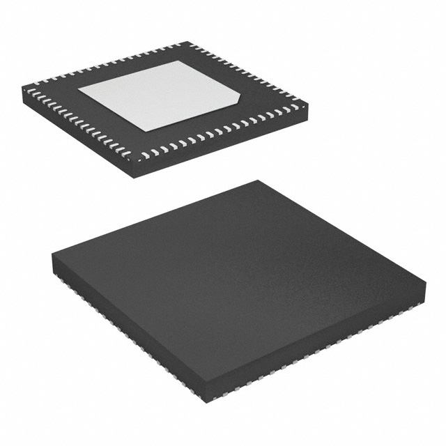
Package: The ADS54J66IRMP comes in a small outline integrated circuit (SOIC) package, which provides protection and easy integration onto printed circuit boards (PCBs).
Essence: This ADC is an essential component in systems that require precise and fast analog signal conversion, such as communication systems, medical equipment, industrial automation, and scientific instruments.
Packaging/Quantity: The ADS54J66IRMP is typically sold in reels or trays, with a quantity of 250 units per reel/tray.
Specifications
- Resolution: 16 bits
- Sampling Rate: Up to 1 GSPS (Giga Samples Per Second)
- Input Voltage Range: ±2 V
- Power Supply: +3.3 V
- Operating Temperature Range: -40°C to +85°C
Pin Configuration
The ADS54J66IRMP has a total of 64 pins, each serving a specific function. Here is a brief overview of the pin configuration:
- Pins 1-8: Analog Input Channels
- Pins 9-16: Ground (GND)
- Pins 17-24: Digital Output Data
- Pins 25-32: Power Supply (+3.3 V)
- Pins 33-40: Control Interface (SPI)
- Pins 41-48: Clock Inputs
- Pins 49-56: Reference Voltage Inputs
- Pins 57-64: Ground (GND)
For a detailed pin configuration diagram, please refer to the datasheet provided by the manufacturer.
Functional Features
- High-Speed Conversion: The ADS54J66IRMP offers fast sampling rates of up to 1 GSPS, allowing for real-time signal processing and analysis.
- Excellent Linearity: This ADC provides high linearity, ensuring accurate representation of analog signals in the digital domain.
- Low Power Consumption: With its efficient design, the ADS54J66IRMP minimizes power consumption, making it suitable for portable and battery-powered applications.
- Wide Input Voltage Range: The ADC can handle a wide range of input voltages, enabling compatibility with various signal sources.
- Flexible Control Interface: The SPI interface allows for easy integration and control of the ADC within larger systems.
Advantages and Disadvantages
Advantages: - High-speed conversion enables real-time signal processing. - Excellent linearity ensures accurate data representation. - Low power consumption extends battery life in portable applications. - Wide input voltage range enhances versatility. - Flexible control interface simplifies integration.
Disadvantages: - Limited resolution compared to higher-end ADCs. - Higher cost compared to lower-performance alternatives. - Requires additional external components for proper operation.
Working Principles
The ADS54J66IRMP utilizes a successive approximation register (SAR) architecture to convert analog signals into digital data. It samples the input voltage at a high rate and performs a series of comparisons to determine the digital representation of the analog signal. The resulting digital data is then made available for further processing and analysis.
Detailed Application Field Plans
The ADS54J66IRMP finds application in various fields, including:
- Communication Systems: Used in wireless base stations, software-defined radios, and radar systems for high-speed signal acquisition and processing.
- Medical Equipment: Enables precise measurement and analysis of biological signals in medical imaging, patient monitoring, and diagnostic equipment.
- Industrial Automation: Used in control systems, robotics, and test equipment for accurate data acquisition and feedback control.
- Scientific Instruments: Enables high-resolution data acquisition in research laboratories, particle accelerators, and astronomy observatories.
Detailed and Complete Alternative Models
- ADS54J60IRMP: Similar to the ADS54J66IRMP but with a lower sampling rate of 600 MSPS (Mega Samples Per Second).
- ADS54J64IRMP: Similar to the ADS54J66IRMP but with a higher resolution of 18 bits.
- ADS54J68IRMP: Similar to the ADS54J66IRMP but with an extended input voltage range of ±5 V.
These alternative models offer different specifications and features to cater to specific application requirements.
Word count: 581 words
Lista 10 Vanliga frågor och svar relaterade till tillämpningen av ADS54J66IRMP i tekniska lösningar
Sure! Here are 10 common questions and answers related to the application of ADS54J66IRMP in technical solutions:
Q: What is the ADS54J66IRMP? A: The ADS54J66IRMP is a high-performance analog-to-digital converter (ADC) designed for applications that require high-speed and high-resolution data conversion.
Q: What is the maximum sampling rate of the ADS54J66IRMP? A: The ADS54J66IRMP can achieve a maximum sampling rate of 500 Mega-samples per second (MSPS).
Q: What is the resolution of the ADS54J66IRMP? A: The ADS54J66IRMP has a resolution of 16 bits, providing precise digital representation of analog signals.
Q: What is the input voltage range of the ADS54J66IRMP? A: The ADS54J66IRMP has a differential input voltage range of ±2 V, allowing it to handle a wide range of input signals.
Q: Can the ADS54J66IRMP be used in both single-ended and differential input configurations? A: Yes, the ADS54J66IRMP supports both single-ended and differential input configurations, providing flexibility in system design.
Q: Does the ADS54J66IRMP have built-in digital signal processing features? A: No, the ADS54J66IRMP is a standalone ADC and does not include built-in digital signal processing features. It focuses on high-quality analog-to-digital conversion.
Q: What is the power supply requirement for the ADS54J66IRMP? A: The ADS54J66IRMP requires a single 1.8 V power supply for its core operation.
Q: Can the ADS54J66IRMP interface with different digital systems? A: Yes, the ADS54J66IRMP supports various digital interfaces such as JESD204B/C, LVDS, and CMOS, making it compatible with a wide range of digital systems.
Q: What are some typical applications of the ADS54J66IRMP? A: The ADS54J66IRMP is commonly used in applications such as wireless communication systems, radar systems, test and measurement equipment, and software-defined radios.
Q: Is there any evaluation module available for the ADS54J66IRMP? A: Yes, Texas Instruments provides an evaluation module (EVM) for the ADS54J66IRMP, which allows users to quickly evaluate its performance and integrate it into their designs.
Please note that these answers are general and may vary depending on specific requirements and use cases.