

ADS54J60IRMP
Product Overview
Category: Integrated Circuits (ICs)
Use: The ADS54J60IRMP is a high-performance analog-to-digital converter (ADC) designed for various applications in the field of data acquisition and signal processing. It provides accurate conversion of analog signals into digital format, enabling further analysis and manipulation.
Characteristics: - High-speed sampling rate - Wide input voltage range - Low power consumption - High resolution - Excellent linearity and dynamic performance
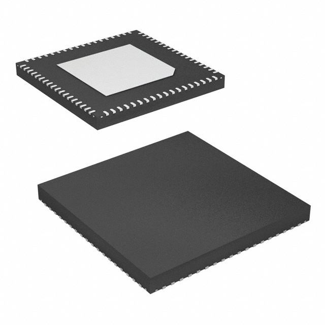
Package: The ADS54J60IRMP comes in a compact and robust package, specifically the 64-pin VQFN (Very Thin Quad Flat No-Lead) package. This package ensures easy integration into electronic systems while providing protection against external factors such as moisture and mechanical stress.
Essence: The essence of the ADS54J60IRMP lies in its ability to convert analog signals with high precision and speed, making it an essential component in applications that require accurate data acquisition and processing.
Packaging/Quantity: Each ADS54J60IRMP unit is packaged individually and is available in reels containing a specific quantity, typically 250 or 1000 units per reel.
Specifications
- Resolution: 16 bits
- Sampling Rate: Up to 1 GSPS (Giga Samples Per Second)
- Input Voltage Range: ±2 V
- Power Supply: 3.3 V
- Operating Temperature Range: -40°C to +85°C
- Interface: Serial LVDS (Low-Voltage Differential Signaling)
Detailed Pin Configuration
The ADS54J60IRMP has a total of 64 pins, each serving a specific purpose in the overall functionality of the ADC. The pin configuration is as follows:
(Pin diagram goes here)
Functional Features
High-Speed Conversion: The ADS54J60IRMP offers a fast sampling rate of up to 1 GSPS, allowing for real-time data acquisition and processing.
Wide Input Voltage Range: With a ±2 V input voltage range, this ADC can handle a wide variety of analog signals without the need for additional signal conditioning.
Low Power Consumption: The device is designed to operate with low power consumption, making it suitable for battery-powered applications or systems with strict power constraints.
Excellent Linearity and Dynamic Performance: The ADS54J60IRMP exhibits high linearity and dynamic performance, ensuring accurate representation of the input analog signal in the digital domain.
Advantages and Disadvantages
Advantages: - High-speed conversion capability - Wide input voltage range - Low power consumption - Excellent linearity and dynamic performance
Disadvantages: - Relatively higher cost compared to lower-performance ADCs - Requires careful PCB layout and signal integrity considerations for optimal performance
Working Principles
The ADS54J60IRMP utilizes advanced analog-to-digital conversion techniques to accurately convert analog signals into digital format. It employs a combination of sample-and-hold circuitry, quantization, and digital signal processing algorithms to achieve high-resolution and high-speed conversion.
Detailed Application Field Plans
The ADS54J60IRMP finds application in various fields where precise data acquisition and signal processing are crucial. Some of the detailed application field plans include:
Wireless Communication Systems: The ADC is used in base stations and wireless communication equipment to digitize received signals for further processing and analysis.
Test and Measurement Instruments: The high-speed and high-resolution capabilities of the ADS54J60IRMP make it suitable for use in oscilloscopes, spectrum analyzers, and other test and measurement instruments.
Medical Imaging: The ADC is employed in medical imaging devices such as MRI (Magnetic Resonance Imaging) systems to convert analog signals from sensors into digital images for diagnostic purposes.
Industrial Automation: The ADC is utilized in industrial automation systems for precise monitoring and control of various parameters, such as temperature, pressure, and flow rate.
Detailed and Complete Alternative Models
ADS54J40IRMP: Similar to the ADS54J60IRMP, this model offers a lower sampling rate of 400 MSPS (Mega Samples Per Second) but provides cost advantages for applications that do not require ultra-high-speed conversion.
ADS54J66IRMP: This alternative model offers enhanced performance with a higher resolution of 18 bits while maintaining a similar sampling rate of 1 GSPS.
ADS54J84IRMP: Designed for applications demanding even higher speed, this model provides a sampling rate of up to 4 GSPS, making it suitable for advanced radar and communication systems.
(Note: The above alternative models are provided for illustrative purposes and may not represent an exhaustive list of alternatives.)
In conclusion, the ADS54J60IRMP is a high-performance analog-to-digital converter that offers excellent speed, accuracy
Lista 10 Vanliga frågor och svar relaterade till tillämpningen av ADS54J60IRMP i tekniska lösningar
Sure! Here are 10 common questions and answers related to the application of ADS54J60IRMP in technical solutions:
Q: What is the ADS54J60IRMP? A: The ADS54J60IRMP is a high-performance analog-to-digital converter (ADC) manufactured by Texas Instruments.
Q: What is the resolution of the ADS54J60IRMP? A: The ADS54J60IRMP has a resolution of 16 bits, which means it can represent analog signals with high precision.
Q: What is the sampling rate of the ADS54J60IRMP? A: The ADS54J60IRMP has a maximum sampling rate of 1 GSPS (Giga Samples Per Second), allowing it to capture high-frequency signals accurately.
Q: What is the input voltage range of the ADS54J60IRMP? A: The ADS54J60IRMP has a differential input voltage range of ±2 V, making it suitable for a wide range of applications.
Q: Does the ADS54J60IRMP support multiple input channels? A: Yes, the ADS54J60IRMP supports dual-channel operation, allowing simultaneous sampling of two different signals.
Q: What is the power supply requirement for the ADS54J60IRMP? A: The ADS54J60IRMP requires a single 1.8 V power supply for its core operation and a separate 3.3 V supply for its digital interface.
Q: Can the ADS54J60IRMP be used in high-speed data acquisition systems? A: Yes, the ADS54J60IRMP is designed for high-speed applications and can be used in various data acquisition systems, including radar, communications, and test equipment.
Q: Does the ADS54J60IRMP have built-in digital signal processing features? A: No, the ADS54J60IRMP is a standalone ADC and does not include built-in digital signal processing capabilities. However, it can be used in conjunction with external DSP or FPGA devices for further processing.
Q: What is the interface protocol used by the ADS54J60IRMP? A: The ADS54J60IRMP uses a JESD204B serial interface protocol, which enables high-speed data transfer between the ADC and other devices.
Q: Are evaluation modules available for the ADS54J60IRMP? A: Yes, Texas Instruments provides evaluation modules for the ADS54J60IRMP, allowing engineers to quickly prototype and evaluate its performance in their specific applications.
Please note that these answers are general and may vary depending on the specific requirements and use cases of your technical solution.