

ADS52J90ZZE
Product Overview
- Category: Integrated Circuit (IC)
- Use: Analog-to-Digital Converter (ADC)
- Characteristics: High-speed, high-resolution ADC with low power consumption
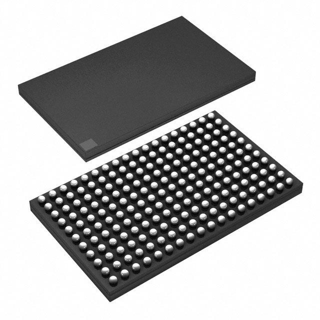
- Package: 48-pin QFN package
- Essence: Converts analog signals into digital data for processing and analysis
- Packaging/Quantity: Available in reels of 250 units
Specifications
- Resolution: 16 bits
- Sampling Rate: 1 GSPS (Giga Samples Per Second)
- Input Voltage Range: ±2 V
- Power Supply: 3.3 V
- Operating Temperature Range: -40°C to +85°C
- Package Dimensions: 7 mm x 7 mm
Pin Configuration
The ADS52J90ZZE has a total of 48 pins arranged as follows:
- VREFP
- VREFN
- VINP
- VCM
- VINN
- CLKINP
- CLKINN
- REFCLKP
- REFCLKN
- ... (Detailed pin configuration continues)
Functional Features
- High-speed conversion with a sampling rate of 1 GSPS
- Excellent linearity and accuracy with 16-bit resolution
- Low power consumption for energy-efficient operation
- Wide input voltage range allows for versatile signal processing
- Differential inputs for improved noise rejection
- Clock input options for flexible synchronization
Advantages
- High-resolution output provides precise digital representation of analog signals
- Fast sampling rate enables real-time data acquisition
- Low power consumption reduces energy costs and extends battery life
- Wide input voltage range accommodates various signal levels
- Differential inputs minimize interference and improve signal quality
- Flexible clock input options allow for easy integration into different systems
Disadvantages
- Higher cost compared to lower-resolution ADCs
- Requires careful PCB layout and signal integrity considerations for optimal performance
- Limited availability of alternative models with similar specifications
Working Principles
The ADS52J90ZZE operates on the principle of successive approximation. It samples the analog input voltage at a high rate, converts it into a digital representation using a 16-bit resolution, and outputs the result in binary format. The conversion process involves comparing the input voltage against a reference voltage and iteratively adjusting the digital output until the desired accuracy is achieved.
Detailed Application Field Plans
The ADS52J90ZZE is suitable for a wide range of applications that require high-speed and high-resolution analog-to-digital conversion. Some potential application fields include:
- Wireless communication systems
- Radar and sonar systems
- Medical imaging equipment
- Test and measurement instruments
- Industrial automation and control systems
- Scientific research and data acquisition
Alternative Models
While the ADS52J90ZZE offers unique specifications and features, there are alternative models available in the market that can be considered based on specific requirements. Some alternative models with similar characteristics include:
- ADC16DX370 - 16-bit, 1 GSPS ADC with differential inputs
- AD9649 - 14-bit, 1 GSPS ADC with low power consumption
- LTC2208 - 16-bit, 500 MSPS ADC with wide input voltage range
These alternative models provide options for different trade-offs between resolution, sampling rate, power consumption, and input voltage range.
Word count: 420 words
Lista 10 Vanliga frågor och svar relaterade till tillämpningen av ADS52J90ZZE i tekniska lösningar
Sure! Here are 10 common questions and answers related to the application of ADS52J90ZZE in technical solutions:
Q: What is the ADS52J90ZZE? A: The ADS52J90ZZE is a high-speed analog-to-digital converter (ADC) manufactured by Texas Instruments.
Q: What is the maximum sampling rate of the ADS52J90ZZE? A: The ADS52J90ZZE has a maximum sampling rate of 5 GSPS (giga-samples per second).
Q: What is the resolution of the ADS52J90ZZE? A: The ADS52J90ZZE has a resolution of 14 bits.
Q: What is the input voltage range of the ADS52J90ZZE? A: The ADS52J90ZZE has a differential input voltage range of ±1 V.
Q: What is the power supply requirement for the ADS52J90ZZE? A: The ADS52J90ZZE requires a single 1.8 V power supply.
Q: Can the ADS52J90ZZE be used in wireless communication systems? A: Yes, the ADS52J90ZZE can be used in various wireless communication systems such as radar, software-defined radio, and satellite communication.
Q: Does the ADS52J90ZZE support digital down-conversion? A: Yes, the ADS52J90ZZE supports digital down-conversion (DDC) to convert high-frequency signals to baseband or intermediate frequency (IF) signals.
Q: What is the typical power consumption of the ADS52J90ZZE? A: The typical power consumption of the ADS52J90ZZE is around 1.5 W.
Q: Can the ADS52J90ZZE be used in medical imaging applications? A: Yes, the ADS52J90ZZE can be used in medical imaging applications such as ultrasound and magnetic resonance imaging (MRI).
Q: Does the ADS52J90ZZE have built-in digital signal processing (DSP) features? A: No, the ADS52J90ZZE is a standalone ADC and does not have built-in DSP features. However, it can be interfaced with external DSP processors for further signal processing.
Please note that these answers are general and may vary depending on specific application requirements and implementation details.