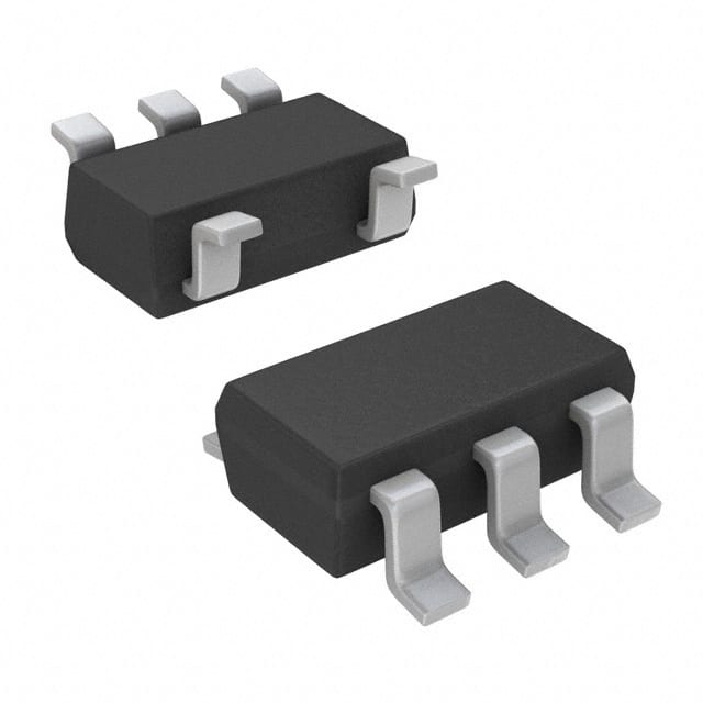
Encyclopedia Entry: 74LVC1G125DCKRG4
Product Overview
Category
The 74LVC1G125DCKRG4 belongs to the category of integrated circuits (ICs) and specifically falls under the family of logic gates.
Use
This product is commonly used in digital electronics for signal amplification, buffering, and level shifting purposes. It serves as a single gate buffer with an output enable control.
Characteristics
- Low-voltage CMOS technology
- High-speed operation
- Wide operating voltage range
- Schmitt-trigger action on inputs
- Balanced propagation delays
- Symmetrical output impedance
Package
The 74LVC1G125DCKRG4 is available in a small SOT-353 package, which is a surface-mount package with three leads.
Essence
The essence of this product lies in its ability to provide reliable signal buffering and level shifting capabilities in a compact form factor.
Packaging/Quantity
The 74LVC1G125DCKRG4 is typically packaged in reels or tape and reel packaging, with a quantity of 3000 units per reel.
Specifications
- Supply Voltage Range: 1.65V to 5.5V
- Input Voltage Range: -0.5V to VCC + 0.5V
- Output Voltage Range: 0V to VCC
- Operating Temperature Range: -40°C to +125°C
- Maximum Propagation Delay: 4.3ns at 3.3V supply voltage
Detailed Pin Configuration
The 74LVC1G125DCKRG4 has the following pin configuration:
____
OE   |    |
I/O  |    |
GND  |    |
VCC  |____|
- OE: Output Enable
- I/O: Input/Output
- GND: Ground
- VCC: Power Supply
Functional Features
The key functional features of the 74LVC1G125DCKRG4 include:
- Output enable control for tri-state operation
- Schmitt-trigger inputs for noise immunity
- High-speed operation for efficient signal processing
- Wide operating voltage range for compatibility with various systems
Advantages and Disadvantages
Advantages
- Compact size and surface-mount package for space-constrained applications
- Low-voltage operation for reduced power consumption
- Schmitt-trigger action on inputs enhances noise immunity
- Balanced propagation delays ensure reliable signal transmission
Disadvantages
- Limited number of gates in a single package
- Not suitable for high-power applications due to low voltage operation
Working Principles
The 74LVC1G125DCKRG4 operates based on complementary metal-oxide-semiconductor (CMOS) technology. It utilizes a combination of transistors and logic gates to amplify and buffer digital signals. The output enable control allows for tri-state operation, enabling the device to drive multiple loads or be disconnected from the bus.
Detailed Application Field Plans
The 74LVC1G125DCKRG4 finds applications in various fields, including but not limited to:
- Consumer electronics: Used in smartphones, tablets, and portable devices for level shifting and buffering signals.
- Industrial automation: Employed in control systems and sensors for signal amplification and interfacing.
- Automotive electronics: Integrated into automotive modules for signal conditioning and level shifting.
- Communication systems: Utilized in networking equipment and data transmission devices for signal integrity maintenance.
Detailed and Complete Alternative Models
Some alternative models that offer similar functionality to the 74LVC1G125DCKRG4 are:
- SN74LVC1G125DBVR - SOT-23 package, 3.3V supply voltage
- MC74LVC1G125DR2G - SOT-23 package, 1.65V to 5.5V supply voltage range
- TC7SZ125FU - SOT-353 package, 1.65V to 5.5V supply voltage range
These alternatives can be considered based on specific application requirements and availability.
In conclusion, the 74LVC1G125DCKRG4 is a versatile logic gate buffer that offers high-speed operation, low-voltage compatibility, and reliable signal amplification. Its compact size and wide operating voltage range make it suitable for various digital electronics applications across different industries.
Lista 10 Vanliga frågor och svar relaterade till tillämpningen av 74LVC1G125DCKRG4 i tekniska lösningar
Sure! Here are 10 common questions and answers related to the application of 74LVC1G125DCKRG4 in technical solutions:
Q1: What is the 74LVC1G125DCKRG4? A1: The 74LVC1G125DCKRG4 is a single bus buffer gate with 3-state output, designed for low-voltage (1.65V to 5.5V) applications.
Q2: What is the purpose of the 74LVC1G125DCKRG4? A2: The purpose of this IC is to provide buffering and level shifting capabilities for digital signals in various electronic circuits.
Q3: What are the key features of the 74LVC1G125DCKRG4? A3: Some key features include high-speed operation, low power consumption, wide voltage range, and 3-state outputs.
Q4: What is the maximum operating frequency of the 74LVC1G125DCKRG4? A4: The maximum operating frequency of this IC is typically around 400 MHz.
Q5: Can the 74LVC1G125DCKRG4 be used with both CMOS and TTL logic levels? A5: Yes, it is compatible with both CMOS and TTL logic levels, making it versatile for different applications.
Q6: How many inputs and outputs does the 74LVC1G125DCKRG4 have? A6: It has one input and one output, along with an enable pin for 3-state control.
Q7: What is the output drive capability of the 74LVC1G125DCKRG4? A7: The output drive capability is typically 32 mA, allowing it to drive moderate loads.
Q8: Can the 74LVC1G125DCKRG4 be used in bidirectional applications? A8: No, it is a unidirectional buffer and cannot be used for bidirectional communication.
Q9: What is the power supply voltage range for the 74LVC1G125DCKRG4? A9: The power supply voltage range is from 1.65V to 5.5V, making it suitable for low-voltage applications.
Q10: What are some typical applications of the 74LVC1G125DCKRG4? A10: Some typical applications include level shifting, signal buffering, clock distribution, and interfacing between different logic families.
Please note that these answers are general and may vary depending on specific datasheet specifications and application requirements.


