

74AVC16722DGGRE4
Basic Information Overview
- Category: Integrated Circuit (IC)
- Use: Digital Logic Device
- Characteristics: High-speed, Low-power, Dual Supply Voltage
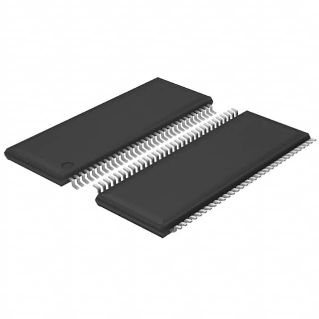
- Package: TSSOP (Thin Shrink Small Outline Package)
- Essence: Data Buffer/Driver
- Packaging/Quantity: Tape and Reel, 2500 units per reel
Specifications
- Number of Inputs: 16
- Number of Outputs: 16
- Supply Voltage Range: 1.2V to 3.6V
- Operating Temperature Range: -40°C to +85°C
- Output Drive Capability: ±24mA
- Propagation Delay Time: 1.5ns (typical)
Detailed Pin Configuration
The 74AVC16722DGGRE4 IC has a total of 48 pins. The pin configuration is as follows:
- A1
- Y1
- B1
- Y2
- A2
- Y3
- B2
- Y4
- A3
- Y5
- B3
- Y6
- A4
- Y7
- B4
- Y8
- GND
- VCCB
- A5
- Y9
- B5
- Y10
- A6
- Y11
- B6
- Y12
- A7
- Y13
- B7
- Y14
- A8
- Y15
- B8
- Y16
- GND
- VCCA
- A9
- Y17
- B9
- Y18
- A10
- Y19
- B10
- Y20
- A11
- Y21
- B11
- Y22
Functional Features
- High-speed operation allows for efficient data transfer.
- Low-power consumption makes it suitable for battery-powered devices.
- Dual supply voltage compatibility enables flexible integration into various systems.
- 3-state outputs provide flexibility in connecting multiple devices.
Advantages and Disadvantages
Advantages: - High-speed operation facilitates fast data processing. - Low-power consumption extends battery life in portable applications. - Dual supply voltage compatibility enhances system design flexibility. - 3-state outputs allow for easy connection with other devices.
Disadvantages: - Limited number of inputs and outputs restricts the complexity of circuits that can be implemented. - Propagation delay time may affect real-time applications requiring immediate response.
Working Principles
The 74AVC16722DGGRE4 is a data buffer/driver IC designed to amplify and transmit digital signals. It operates by receiving input signals on its 16 input pins and providing amplified output signals on the corresponding 16 output pins. The IC is powered by dual supply voltages, allowing it to interface with different logic families. The 3-state outputs enable multiple devices to share a common bus without interference.
Detailed Application Field Plans
The 74AVC16722DGGRE4 IC finds application in various fields, including: 1. Communication Systems: Used for signal buffering and driving in high-speed data transmission. 2. Computer Peripherals: Enables efficient data transfer between different components. 3. Industrial Automation: Facilitates reliable communication between control units and sensors/actuators. 4. Automotive Electronics: Supports data buffering and driving in automotive communication networks. 5. Consumer Electronics: Used in devices such as smartphones, tablets, and gaming consoles for signal amplification and transmission.
Detailed and Complete Alternative Models
- SN74AVC16722DGGR: Similar specifications and pin configuration, offered by Texas Instruments.
- MC74AVC16722DG: Comparable features and functionality, manufactured by ON Semiconductor.
- 74VCX16244MTDX: Alternative IC with similar characteristics, available from Fairchild Semiconductor.
(Note: The above alternative models are provided as examples and may not cover the entire range of alternatives available in the market.)
Word count: 510 words
Lista 10 Vanliga frågor och svar relaterade till tillämpningen av 74AVC16722DGGRE4 i tekniska lösningar
Sure! Here are 10 common questions and answers related to the application of 74AVC16722DGGRE4 in technical solutions:
1. What is the 74AVC16722DGGRE4? - The 74AVC16722DGGRE4 is a 16-bit buffer/driver with 3-state outputs, designed for high-speed applications.
2. What is the maximum operating voltage for this device? - The maximum operating voltage for the 74AVC16722DGGRE4 is 3.6V.
3. What is the typical output current capability of this buffer/driver? - The typical output current capability of the 74AVC16722DGGRE4 is ±24mA.
4. Can I use this device for level shifting between different voltage domains? - Yes, the 74AVC16722DGGRE4 can be used for level shifting between different voltage domains as long as the voltage levels are within its specified range.
5. Is this device suitable for high-speed data transmission? - Yes, the 74AVC16722DGGRE4 is designed for high-speed applications and can support data transmission rates up to several hundred megabits per second.
6. Does this buffer/driver have built-in ESD protection? - Yes, the 74AVC16722DGGRE4 has built-in ESD protection, which helps protect the device from electrostatic discharge events.
7. Can I use this device in automotive applications? - Yes, the 74AVC16722DGGRE4 is qualified for automotive applications and meets the necessary standards and requirements.
8. What is the power supply voltage range for this device? - The power supply voltage range for the 74AVC16722DGGRE4 is typically from 1.2V to 3.6V.
9. Does this buffer/driver have a thermal shutdown feature? - No, the 74AVC16722DGGRE4 does not have a thermal shutdown feature.
10. Can I use this device in industrial control systems? - Yes, the 74AVC16722DGGRE4 can be used in various industrial control systems where high-speed buffering or level shifting is required.
Please note that these answers are general and may vary depending on the specific datasheet and application requirements.