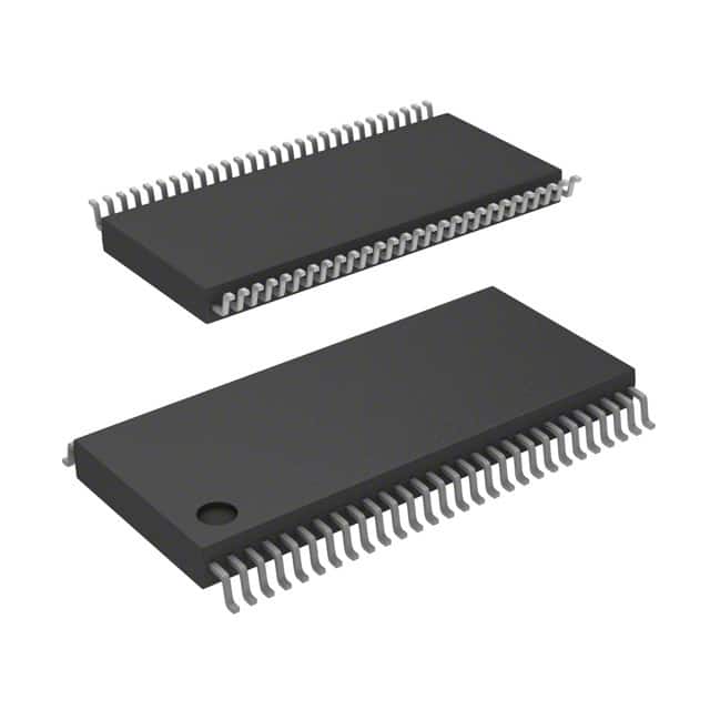
Encyclopedia Entry: 74ALVCH16409DGGRE4
Product Overview
Category
The 74ALVCH16409DGGRE4 belongs to the category of integrated circuits (ICs). Specifically, it falls under the category of digital logic ICs.
Use
This product is primarily used for data manipulation and signal processing in various electronic devices and systems. It is commonly employed in applications that require high-speed data transfer and efficient data storage.
Characteristics
- High-speed operation: The 74ALVCH16409DGGRE4 is designed to operate at high clock frequencies, making it suitable for time-critical applications.
- Low power consumption: This IC incorporates advanced power-saving techniques, ensuring efficient energy usage.
- Wide voltage range: It can operate within a wide supply voltage range, providing flexibility in different electronic systems.
- ESD protection: The 74ALVCH16409DGGRE4 offers built-in electrostatic discharge (ESD) protection, safeguarding the circuitry from potential damage.
Package
The 74ALVCH16409DGGRE4 is available in a small form factor package known as TSSOP (Thin Shrink Small Outline Package). This package type allows for compact integration into electronic devices while maintaining ease of assembly.
Essence
The essence of the 74ALVCH16409DGGRE4 lies in its ability to efficiently process and manipulate digital data, enabling seamless communication and control within electronic systems.
Packaging/Quantity
Typically, this product is supplied in reels containing multiple units. The exact quantity per reel may vary depending on the manufacturer's specifications.
Specifications
- Logic family: ALVCH
- Number of bits: 16
- Input/output voltage levels: 3.3V
- Supply voltage range: 1.65V to 3.6V
- Operating temperature range: -40°C to 85°C
- Input/output type: Non-inverting
Detailed Pin Configuration
The 74ALVCH16409DGGRE4 features a total of 56 pins, each serving a specific function. The pin configuration is as follows:
- Pin 1: Output Q0
- Pin 2: Output Q1
- Pin 3: Output Q2
- Pin 4: Output Q3
- Pin 5: Output Q4
- Pin 6: Output Q5
- Pin 7: Output Q6
- Pin 8: Output Q7
- Pin 9: Output Q8
- Pin 10: Output Q9
- Pin 11: Output Q10
- Pin 12: Output Q11
- Pin 13: Output Q12
- Pin 14: Output Q13
- Pin 15: Output Q14
- Pin 16: Output Q15
- Pin 17: GND (Ground)
- Pin 18: Output Enable (OE)
- Pin 19: Clock (CLK)
- Pin 20: Data Input D0
- Pin 21: Data Input D1
- Pin 22: Data Input D2
- Pin 23: Data Input D3
- Pin 24: Data Input D4
- Pin 25: Data Input D5
- Pin 26: Data Input D6
- Pin 27: Data Input D7
- Pin 28: Data Input D8
- Pin 29: Data Input D9
- Pin 30: Data Input D10
- Pin 31: Data Input D11
- Pin 32: Data Input D12
- Pin 33: Data Input D13
- Pin 34: Data Input D14
- Pin 35: Data Input D15
- Pin 36: VCC (Supply Voltage)
Note: The remaining pins are not listed here for brevity.
Functional Features
The 74ALVCH16409DGGRE4 offers the following functional features:
- 16-bit data storage: It can store and manipulate 16 bits of digital data simultaneously.
- Non-inverting outputs: The outputs are non-inverting, ensuring compatibility with other digital logic circuits.
- Output enable control: The OE pin allows for enabling or disabling the outputs, providing flexibility in data flow control.
- High-speed operation: This IC is designed to operate at high clock frequencies, facilitating rapid data processing.
- Low power consumption: The 74ALVCH16409DGGRE4 incorporates power-saving techniques, minimizing energy consumption.
Advantages and Disadvantages
Advantages
- High-speed operation enables efficient data processing
Lista 10 Vanliga frågor och svar relaterade till tillämpningen av 74ALVCH16409DGGRE4 i tekniska lösningar
Sure! Here are 10 common questions and answers related to the application of 74ALVCH16409DGGRE4 in technical solutions:
Q: What is the function of the 74ALVCH16409DGGRE4? A: The 74ALVCH16409DGGRE4 is a 16-bit universal bus transceiver with 3-state outputs.
Q: What voltage levels does the 74ALVCH16409DGGRE4 support? A: The 74ALVCH16409DGGRE4 supports both 3.3V and 5V voltage levels.
Q: Can the 74ALVCH16409DGGRE4 be used for bidirectional data transfer? A: Yes, the 74ALVCH16409DGGRE4 can be used for bidirectional data transfer.
Q: How many inputs and outputs does the 74ALVCH16409DGGRE4 have? A: The 74ALVCH16409DGGRE4 has 16 inputs and 16 outputs.
Q: What is the maximum operating frequency of the 74ALVCH16409DGGRE4? A: The maximum operating frequency of the 74ALVCH16409DGGRE4 is typically around 400 MHz.
Q: Does the 74ALVCH16409DGGRE4 have built-in ESD protection? A: Yes, the 74ALVCH16409DGGRE4 has built-in ESD protection on all inputs and outputs.
Q: Can the 74ALVCH16409DGGRE4 be used in high-speed data communication applications? A: Yes, the 74ALVCH16409DGGRE4 is suitable for high-speed data communication applications.
Q: What is the power supply voltage range for the 74ALVCH16409DGGRE4? A: The power supply voltage range for the 74ALVCH16409DGGRE4 is typically between 2.3V and 3.6V.
Q: Does the 74ALVCH16409DGGRE4 have any special features for bus interfacing? A: Yes, the 74ALVCH16409DGGRE4 has a direction control pin (DIR) that allows easy bus interfacing.
Q: Is the 74ALVCH16409DGGRE4 available in different package options? A: Yes, the 74ALVCH16409DGGRE4 is available in various package options, such as TSSOP and VFBGA.
Please note that these answers are general and may vary depending on the specific datasheet and application requirements.


