

74LX1GU04STR
Product Overview
- Category: Integrated Circuit (IC)
- Use: Logic Gate
- Characteristics: Low-power, single-gate inverter
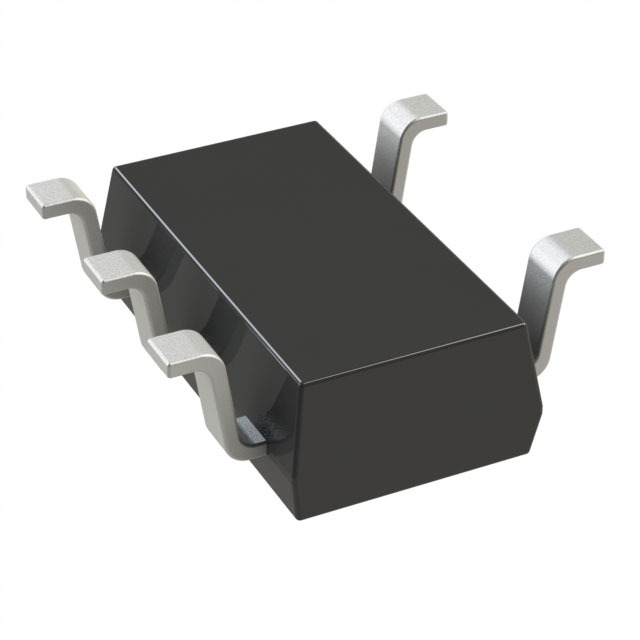
- Package: Small Outline Transistor (SOT) package
- Essence: Logic gate with one input and one output
- Packaging/Quantity: Tape and reel packaging, available in various quantities
Specifications
- Supply Voltage Range: 1.65V to 5.5V
- Input Voltage Range: 0V to VCC
- Output Voltage Range: 0V to VCC
- Operating Temperature Range: -40°C to +85°C
- Propagation Delay Time: 4.5ns (typical)
- Maximum Quiescent Current: 1μA (at 5.5V)
Detailed Pin Configuration
The 74LX1GU04STR has a total of 5 pins:
- GND (Ground): Connected to the ground reference voltage.
- IN (Input): Receives the logic signal to be inverted.
- OUT (Output): Provides the inverted logic signal.
- NC (No Connection): Unused pin, not connected internally.
- VCC (Power Supply): Connected to the positive supply voltage.
Functional Features
- Single-gate inverter: Converts the input logic level to its complement.
- Low-power consumption: Operates at very low quiescent current levels.
- Wide supply voltage range: Can be powered by various voltage sources.
- Fast propagation delay: Provides quick response times for signal inversion.
Advantages and Disadvantages
Advantages: - Compact size and small footprint. - Low power consumption makes it suitable for battery-powered devices. - Wide supply voltage range allows for versatile applications. - Fast propagation delay ensures efficient signal inversion.
Disadvantages: - Limited functionality as a single-gate inverter. - Not suitable for complex logic operations requiring multiple gates.
Working Principles
The 74LX1GU04STR is based on complementary metal-oxide-semiconductor (CMOS) technology. It utilizes a combination of NMOS and PMOS transistors to achieve the logic inversion function. When the input voltage is low, the NMOS transistor conducts, allowing current to flow from the positive supply voltage to the ground. This results in a low output voltage. Conversely, when the input voltage is high, the PMOS transistor conducts, connecting the output to the positive supply voltage, resulting in a high output voltage.
Detailed Application Field Plans
The 74LX1GU04STR can be used in various applications, including but not limited to: - Digital logic circuits - Microcontrollers and microprocessors - Communication systems - Consumer electronics - Industrial automation
Detailed and Complete Alternative Models
Some alternative models that offer similar functionality to the 74LX1GU04STR include: - 74HC04: High-speed CMOS hex inverter - SN74LS04: Low-power Schottky hex inverter - CD4069UB: CMOS hex inverter with buffered outputs - MC74VHC1GU04: Single-gate CMOS inverter with Schmitt-trigger inputs
These alternatives provide different features and specifications, allowing users to choose the most suitable option for their specific requirements.
Word count: 346 words
Lista 10 Vanliga frågor och svar relaterade till tillämpningen av 74LX1GU04STR i tekniska lösningar
Sure! Here are 10 common questions and answers related to the application of 74LX1GU04STR in technical solutions:
Q1: What is the 74LX1GU04STR? A1: The 74LX1GU04STR is a single unbuffered inverter gate IC (Integrated Circuit) that is commonly used in digital logic circuits.
Q2: What is the voltage supply range for the 74LX1GU04STR? A2: The voltage supply range for the 74LX1GU04STR is typically between 1.65V and 5.5V.
Q3: What is the maximum output current of the 74LX1GU04STR? A3: The maximum output current of the 74LX1GU04STR is around 32mA.
Q4: Can the 74LX1GU04STR be used as a level shifter? A4: Yes, the 74LX1GU04STR can be used as a level shifter to convert signals from one voltage level to another.
Q5: How many inverters are there in the 74LX1GU04STR? A5: The 74LX1GU04STR contains a single inverter gate.
Q6: What is the propagation delay of the 74LX1GU04STR? A6: The propagation delay of the 74LX1GU04STR is typically around 7.5ns.
Q7: Can the 74LX1GU04STR be used in high-speed applications? A7: Yes, the 74LX1GU04STR can be used in high-speed applications due to its low propagation delay.
Q8: Is the 74LX1GU04STR compatible with other logic families? A8: Yes, the 74LX1GU04STR is compatible with various logic families such as CMOS, TTL, and LVTTL.
Q9: What is the package type of the 74LX1GU04STR? A9: The 74LX1GU04STR is available in a small SOT-23 package.
Q10: Can the 74LX1GU04STR be used in battery-powered applications? A10: Yes, the 74LX1GU04STR can be used in battery-powered applications due to its low voltage supply range and low power consumption.
Please note that these answers are general and may vary depending on specific datasheet specifications or application requirements.