

AAT4910IJS-T1
Product Overview
Category
AAT4910IJS-T1 belongs to the category of integrated circuits (ICs).
Use
This IC is commonly used in electronic devices for voltage regulation and power management.
Characteristics
- Voltage regulation capabilities
- Power management features
- Compact size
- High efficiency
- Low power consumption
Package
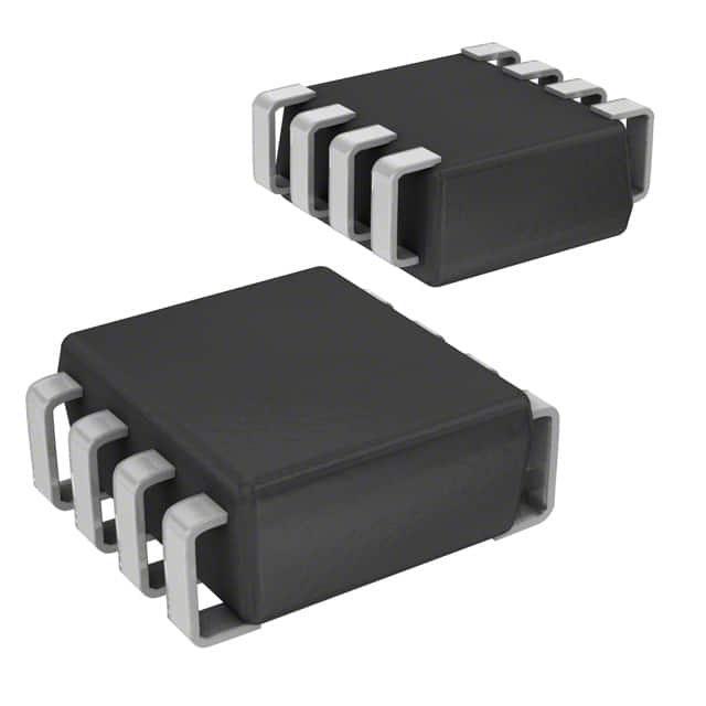
AAT4910IJS-T1 is available in a small outline package (SOP) format.
Essence
The essence of AAT4910IJS-T1 lies in its ability to regulate voltage and manage power efficiently, making it an essential component in various electronic devices.
Packaging/Quantity
This IC is typically packaged in reels or tubes, with a quantity of 2500 units per reel/tube.
Specifications
- Input Voltage Range: 2.7V to 5.5V
- Output Voltage Range: Adjustable from 0.6V to VIN
- Maximum Output Current: 1.5A
- Quiescent Current: 60µA (typical)
- Switching Frequency: 1.2MHz (typical)
- Operating Temperature Range: -40°C to +85°C
Detailed Pin Configuration
AAT4910IJS-T1 has the following pin configuration:
- VIN: Input voltage pin
- GND: Ground pin
- EN: Enable pin
- FB: Feedback pin
- SW: Switch pin
- VOUT: Output voltage pin
Functional Features
- Wide input voltage range allows compatibility with various power sources.
- Adjustable output voltage enables flexibility in different applications.
- High output current capability supports power-hungry devices.
- Low quiescent current minimizes power consumption during standby mode.
- High switching frequency ensures efficient power conversion.
- Enable pin allows for easy control of the IC's operation.
Advantages and Disadvantages
Advantages
- Efficient voltage regulation and power management
- Compact size for space-constrained applications
- Wide input voltage range for versatility
- Adjustable output voltage for flexibility
- Low power consumption during standby mode
Disadvantages
- Limited maximum output current compared to some other ICs in the same category
- Relatively high switching frequency may introduce electromagnetic interference in sensitive applications
Working Principles
AAT4910IJS-T1 operates based on a switching regulator topology. It uses an internal power MOSFET to regulate the output voltage by adjusting the duty cycle of the switching signal. This enables efficient conversion of input voltage to the desired output voltage, while minimizing power losses.
Detailed Application Field Plans
AAT4910IJS-T1 finds applications in various electronic devices, including but not limited to: - Mobile phones - Tablets - Portable media players - Digital cameras - Wireless communication devices - Battery-powered devices
Detailed and Complete Alternative Models
Some alternative models that offer similar functionality to AAT4910IJS-T1 include: - AAT4910IJT-T1 - AAT4910IKS-T1 - AAT4910IKT-T1 - AAT4910ILS-T1 - AAT4910ILT-T1
These alternative models provide comparable voltage regulation and power management capabilities, allowing designers to choose the most suitable option for their specific application requirements.
Word count: 446 words
Lista 10 Vanliga frågor och svar relaterade till tillämpningen av AAT4910IJS-T1 i tekniska lösningar
Sure! Here are 10 common questions and answers related to the application of AAT4910IJS-T1 in technical solutions:
Q1: What is the AAT4910IJS-T1? A1: The AAT4910IJS-T1 is a specific model of integrated circuit (IC) that is commonly used in technical solutions.
Q2: What is the purpose of the AAT4910IJS-T1? A2: The AAT4910IJS-T1 is designed to provide power management and control functions in various electronic devices and systems.
Q3: What are the key features of the AAT4910IJS-T1? A3: Some key features of the AAT4910IJS-T1 include low voltage operation, high efficiency, overcurrent protection, thermal shutdown, and adjustable output voltage.
Q4: In which applications can the AAT4910IJS-T1 be used? A4: The AAT4910IJS-T1 can be used in a wide range of applications such as smartphones, tablets, portable media players, digital cameras, and other battery-powered devices.
Q5: How does the AAT4910IJS-T1 help in power management? A5: The AAT4910IJS-T1 helps in power management by regulating and controlling the voltage levels supplied to different components within a device, ensuring efficient power usage.
Q6: Can the AAT4910IJS-T1 handle multiple power sources? A6: Yes, the AAT4910IJS-T1 is capable of handling multiple power sources, allowing for seamless switching between different power inputs.
Q7: Is the AAT4910IJS-T1 easy to integrate into existing designs? A7: Yes, the AAT4910IJS-T1 is designed to be easily integrated into existing designs, thanks to its compact size and compatibility with standard electronic components.
Q8: Does the AAT4910IJS-T1 have any built-in protection features? A8: Yes, the AAT4910IJS-T1 incorporates various protection features such as overcurrent protection and thermal shutdown to safeguard against potential damage or overheating.
Q9: Can the output voltage of the AAT4910IJS-T1 be adjusted? A9: Yes, the output voltage of the AAT4910IJS-T1 can be adjusted using external components, allowing for customization based on specific requirements.
Q10: Where can I find more information about the AAT4910IJS-T1? A10: You can find more detailed information about the AAT4910IJS-T1 in the datasheet provided by the manufacturer or by visiting their official website.