

RF1001T2D Product Overview
Introduction
The RF1001T2D is a versatile electronic component that belongs to the category of radio frequency (RF) transistors. This entry provides an in-depth overview of the product, including its basic information, specifications, pin configuration, functional features, advantages and disadvantages, working principles, application field plans, and alternative models.
Basic Information Overview
- Category: RF Transistor
- Use: Amplification and signal processing in RF circuits
- Characteristics: High-frequency operation, low noise, and high gain
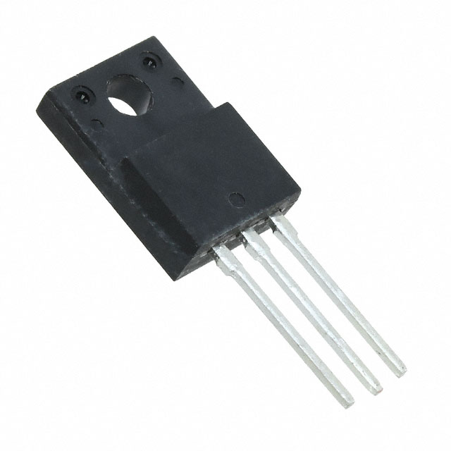
- Package: TO-220
- Essence: Silicon NPN RF Transistor
- Packaging/Quantity: Typically available in reels or tubes containing multiple units
Specifications
- Maximum Power Dissipation: 1.5W
- Collector-Base Voltage (VCBO): 30V
- Collector-Emitter Voltage (VCEO): 20V
- Emitter-Base Voltage (VEBO): 3V
- Collector Current (IC): 0.7A
- Transition Frequency (fT): 800MHz
- Noise Figure: 1dB
Detailed Pin Configuration
The RF1001T2D transistor has three pins: 1. Collector (C): Connected to the positive supply voltage 2. Base (B): Input terminal for controlling the transistor's conductivity 3. Emitter (E): Output terminal for the amplified signal
Functional Features
- High-frequency operation suitable for RF applications
- Low noise figure for improved signal fidelity
- High gain for effective signal amplification
Advantages and Disadvantages
Advantages
- Suitable for high-frequency RF circuits
- Low noise figure enhances signal quality
- Compact TO-220 package for easy integration
Disadvantages
- Limited maximum power dissipation
- Relatively low collector current rating
Working Principles
The RF1001T2D operates based on the principles of bipolar junction transistors. When a small signal is applied to the base terminal, it controls the larger current flowing between the collector and emitter, effectively amplifying the input signal.
Detailed Application Field Plans
The RF1001T2D is commonly used in the following applications: - RF amplifiers - RF oscillators - RF mixers - RF preamplifiers
Detailed and Complete Alternative Models
Some alternative models to the RF1001T2D include: - RF1002T2D - RF1003T2D - RF1004T2D
In conclusion, the RF1001T2D is a valuable RF transistor with specific characteristics and applications in high-frequency RF circuits. Its compact package and high gain make it suitable for various RF amplification and signal processing tasks.
Word Count: 368
Lista 10 Vanliga frågor och svar relaterade till tillämpningen av RF1001T2D i tekniska lösningar
Sure, here are 10 common questions and answers related to the application of RF1001T2D in technical solutions:
Q: What is RF1001T2D? A: RF1001T2D is a high-frequency, low-noise amplifier designed for use in RF and microwave applications.
Q: What is the frequency range of RF1001T2D? A: The frequency range of RF1001T2D is typically from 100 MHz to 1 GHz.
Q: What is the gain of RF1001T2D? A: The gain of RF1001T2D is typically around 20 dB.
Q: What is the noise figure of RF1001T2D? A: The noise figure of RF1001T2D is typically around 2 dB.
Q: What is the input and output impedance of RF1001T2D? A: The input and output impedance of RF1001T2D is typically 50 ohms.
Q: What are the typical applications of RF1001T2D? A: RF1001T2D is commonly used in wireless communication systems, radar systems, and test and measurement equipment.
Q: Is RF1001T2D suitable for use in high-power applications? A: No, RF1001T2D is not designed for high-power applications and may be damaged if subjected to high power levels.
Q: Can RF1001T2D be used in harsh environmental conditions? A: RF1001T2D is not specifically designed for harsh environmental conditions and may require additional protection or enclosure if used in such environments.
Q: What is the operating voltage range of RF1001T2D? A: The operating voltage range of RF1001T2D is typically between 3V and 5V.
Q: Are there any specific layout considerations for using RF1001T2D in a PCB design? A: Yes, proper RF layout techniques should be followed to minimize parasitic effects and ensure optimal performance of RF1001T2D in a PCB design.
I hope these questions and answers are helpful! Let me know if you need further assistance.