

BR25S128FVT-WE2
Product Overview
Category: Integrated Circuit (IC)
Use: Non-volatile Memory
Characteristics: - High-speed data transfer - Low power consumption - Wide operating voltage range - Small form factor
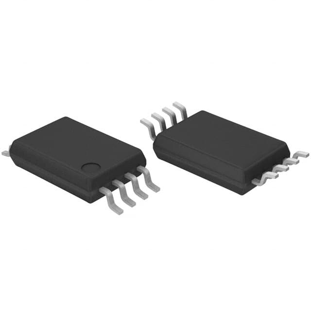
Package: SOP-8 (Small Outline Package)
Essence: The BR25S128FVT-WE2 is a non-volatile memory IC that provides high-speed data transfer and low power consumption. It is commonly used in various electronic devices for storing data.
Packaging/Quantity: The BR25S128FVT-WE2 is typically packaged in reels or tubes, with a quantity of 2500 units per reel/tube.
Specifications
- Memory Capacity: 128 kilobits (16 kilobytes)
- Interface: SPI (Serial Peripheral Interface)
- Operating Voltage Range: 1.7V to 5.5V
- Data Transfer Speed: Up to 10 MHz
- Operating Temperature Range: -40°C to +85°C
- Data Retention: Up to 20 years
- Endurance: Up to 1 million write cycles
Detailed Pin Configuration
The BR25S128FVT-WE2 has a total of 8 pins arranged as follows:
- Chip Select (/CS)
- Serial Clock (SCK)
- Serial Data Input (SI)
- Serial Data Output (SO)
- Write Protect (/WP)
- Hold (/HOLD)
- Ground (GND)
- Power Supply (VCC)
Functional Features
- High-speed data transfer: The BR25S128FVT-WE2 supports data transfer speeds of up to 10 MHz, allowing for efficient read and write operations.
- Low power consumption: With its advanced power management features, the IC minimizes energy usage, making it suitable for battery-powered devices.
- Wide operating voltage range: The IC can operate within a voltage range of 1.7V to 5.5V, providing flexibility in various applications.
- Small form factor: The SOP-8 package ensures a compact size, enabling easy integration into space-constrained designs.
Advantages and Disadvantages
Advantages: - High-speed data transfer - Low power consumption - Wide operating voltage range - Compact size
Disadvantages: - Limited memory capacity (128 kilobits)
Working Principles
The BR25S128FVT-WE2 utilizes the Serial Peripheral Interface (SPI) protocol for communication with the host device. It stores data in non-volatile memory cells, which retain information even when power is disconnected. The IC can be accessed by sending commands through the SPI interface, allowing for read and write operations.
Detailed Application Field Plans
The BR25S128FVT-WE2 is widely used in various electronic devices that require non-volatile memory storage. Some common application fields include:
- Consumer Electronics: Used in smart TVs, set-top boxes, and digital cameras for storing firmware, configuration data, and user settings.
- Automotive: Employed in car infotainment systems, instrument clusters, and navigation systems for data storage and firmware updates.
- Industrial Automation: Utilized in programmable logic controllers (PLCs), industrial sensors, and control systems for storing critical data and program code.
- IoT Devices: Integrated into smart home devices, wearables, and connected appliances for data logging and firmware upgrades.
Detailed and Complete Alternative Models
- BR25A128FJ-WE2: Similar to BR25S128FVT-WE2 but with an I2C interface instead of SPI.
- BR25L128FJ-WE2: Same memory capacity and package as BR25S128FVT-WE2, but optimized for low-power applications.
- BR25H128FJ-WE2: Offers additional hardware security features for enhanced data protection.
(Note: The above alternative models are provided for reference and may have slight variations in specifications and features.)
Word count: 530 words
Lista 10 Vanliga frågor och svar relaterade till tillämpningen av BR25S128FVT-WE2 i tekniska lösningar
Sure! Here are 10 common questions and answers related to the application of BR25S128FVT-WE2 in technical solutions:
Q: What is the capacity of the BR25S128FVT-WE2 memory chip? A: The BR25S128FVT-WE2 has a capacity of 128 kilobits (16 kilobytes).
Q: What is the operating voltage range for this memory chip? A: The operating voltage range for the BR25S128FVT-WE2 is 1.65V to 3.6V.
Q: Can the BR25S128FVT-WE2 be used in industrial applications? A: Yes, the BR25S128FVT-WE2 is suitable for use in various industrial applications.
Q: Does this memory chip support high-speed SPI communication? A: Yes, the BR25S128FVT-WE2 supports high-speed SPI communication up to 5 MHz.
Q: Is the BR25S128FVT-WE2 compatible with both 3.3V and 5V logic levels? A: No, the BR25S128FVT-WE2 is only compatible with 3.3V logic levels.
Q: Can I use this memory chip in automotive electronics applications? A: Yes, the BR25S128FVT-WE2 is designed to meet the requirements of automotive electronics.
Q: Does the BR25S128FVT-WE2 have built-in write protection features? A: Yes, this memory chip provides hardware and software write protection options.
Q: What is the typical endurance of the BR25S128FVT-WE2? A: The typical endurance of this memory chip is 1 million write cycles per sector.
Q: Can I operate the BR25S128FVT-WE2 at high temperatures? A: Yes, the BR25S128FVT-WE2 has an extended temperature range of -40°C to +105°C.
Q: Is the BR25S128FVT-WE2 RoHS compliant? A: Yes, this memory chip is RoHS (Restriction of Hazardous Substances) compliant, ensuring environmental safety.
Please note that these answers are based on general information about the BR25S128FVT-WE2 and may vary depending on specific application requirements.