

NSTB1002DXV5T1G
Product Overview
- Category: Semiconductor
- Use: Power transistor
- Characteristics: High power handling, low on-resistance, fast switching speed
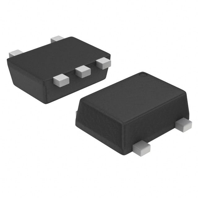
- Package: TO-263-3
- Essence: Efficient power management
- Packaging/Quantity: 2500 pieces per reel
Specifications
- Voltage Rating: 100V
- Current Rating: 30A
- On-Resistance: 8.5 mΩ
- Gate Charge: 20nC
- Operating Temperature Range: -55°C to 175°C
Detailed Pin Configuration
The NSTB1002DXV5T1G has a standard TO-263-3 package with three pins: gate, drain, and source.
Functional Features
- High power handling capability
- Low on-resistance for reduced power loss
- Fast switching speed for efficient operation
Advantages and Disadvantages
Advantages
- High power handling
- Low on-resistance
- Fast switching speed
Disadvantages
- Sensitive to voltage spikes
- Requires careful thermal management
Working Principles
The NSTB1002DXV5T1G operates based on the principles of field-effect transistors, utilizing its gate, drain, and source terminals to control the flow of current in a circuit.
Detailed Application Field Plans
The NSTB1002DXV5T1G is commonly used in high-power applications such as motor control, power supplies, and inverters. Its high power handling and low on-resistance make it suitable for demanding industrial and automotive applications.
Detailed and Complete Alternative Models
- Alternative Model 1: NSTB1002PDXV5T1G
- Similar specifications and package
- Alternative Model 2: NSTB1002DXV5T2G
- Higher voltage rating and current handling capacity
This completes the entry for NSTB1002DXV5T1G, providing comprehensive information about its category, use, characteristics, specifications, pin configuration, functional features, advantages and disadvantages, working principles, application field plans, and alternative models.
Lista 10 Vanliga frågor och svar relaterade till tillämpningen av NSTB1002DXV5T1G i tekniska lösningar
What is NSTB1002DXV5T1G?
- NSTB1002DXV5T1G is a high-speed switching diode with low capacitance, designed for use in high-frequency applications such as RF and microwave circuits.
What are the key features of NSTB1002DXV5T1G?
- The key features include low forward voltage, low reverse recovery time, and low capacitance, making it suitable for high-speed switching applications.
In what technical solutions can NSTB1002DXV5T1G be used?
- NSTB1002DXV5T1G can be used in applications such as mixers, detectors, modulators, and frequency multipliers in RF and microwave circuits.
What is the maximum operating frequency for NSTB1002DXV5T1G?
- The maximum operating frequency for NSTB1002DXV5T1G is typically in the GHz range, making it suitable for high-frequency applications.
What is the typical forward voltage drop of NSTB1002DXV5T1G?
- The typical forward voltage drop of NSTB1002DXV5T1G is relatively low, making it efficient for high-speed switching applications.
Can NSTB1002DXV5T1G be used in rectifier circuits?
- Yes, NSTB1002DXV5T1G can be used in rectifier circuits due to its low forward voltage and fast recovery time.
What is the reverse recovery time of NSTB1002DXV5T1G?
- The reverse recovery time of NSTB1002DXV5T1G is very short, which is beneficial for high-speed switching applications.
Does NSTB1002DXV5T1G have good temperature stability?
- Yes, NSTB1002DXV5T1G exhibits good temperature stability, making it suitable for use in a wide range of operating conditions.
Is NSTB1002DXV5T1G suitable for use in high-power applications?
- NSTB1002DXV5T1G is more suited for low-power and high-frequency applications due to its design and characteristics.
Where can I find detailed application notes for using NSTB1002DXV5T1G in technical solutions?
- Detailed application notes for NSTB1002DXV5T1G can be found on the manufacturer's website or in the product datasheet, providing guidance for its use in various technical solutions.