

NLX3G14AMX1TCG
Product Overview
Category: Integrated Circuit (IC)
Use: The NLX3G14AMX1TCG is a high-performance hex inverter Schmitt trigger IC. It is commonly used in digital logic circuits for signal conditioning and level shifting applications.
Characteristics: - High-speed operation - Wide operating voltage range - Low power consumption - Schmitt trigger input for noise immunity - Small package size for space-constrained designs
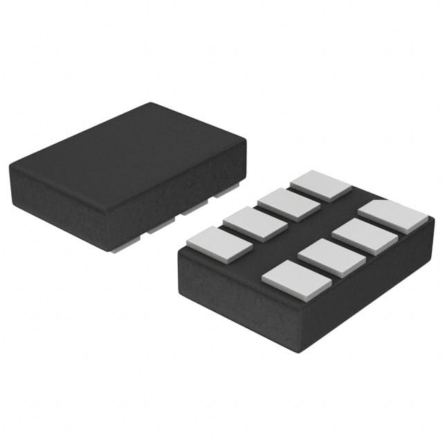
Package: The NLX3G14AMX1TCG is available in a small outline package (SOT-23) which provides ease of integration into various electronic systems.
Essence: This IC serves as a versatile building block for digital circuit design, enabling reliable signal processing and level conversion.
Packaging/Quantity: The NLX3G14AMX1TCG is typically sold in reels containing 3000 units per reel.
Specifications
- Supply Voltage Range: 1.65V to 5.5V
- Input Voltage Range: 0V to Vcc
- Output Voltage Range: 0V to Vcc
- Operating Temperature Range: -40°C to +85°C
- Propagation Delay: 4.5 ns (typical)
- Input Capacitance: 2 pF (typical)
- Output Drive Capability: ±8 mA
Detailed Pin Configuration
The NLX3G14AMX1TCG features a standard SOT-23 package with the following pin configuration:
____
   1 |*    | 6
   2 |     | 5
   3 |_____| 4
Pin Description: 1. Input A 2. Ground (GND) 3. Output Y 4. Output Y 5. Vcc (Supply Voltage) 6. Input B
Functional Features
- Hex inverter with Schmitt trigger inputs
- Converts input logic levels to output logic levels
- Provides hysteresis for noise immunity
- High-speed operation allows for efficient signal processing
- Wide operating voltage range enables compatibility with various systems
Advantages and Disadvantages
Advantages: - High-speed operation enhances overall system performance - Wide operating voltage range increases versatility - Small package size facilitates integration into space-constrained designs - Schmitt trigger input provides noise immunity
Disadvantages: - Limited output drive capability may restrict use in certain applications - Higher power consumption compared to some alternative models
Working Principles
The NLX3G14AMX1TCG operates as a hex inverter with Schmitt trigger inputs. It converts the input logic levels to output logic levels, providing hysteresis for noise immunity. The high-speed operation ensures efficient signal processing, while the wide operating voltage range allows for compatibility with various systems.
Detailed Application Field Plans
The NLX3G14AMX1TCG finds application in various digital logic circuits, including but not limited to: - Signal conditioning - Level shifting - Oscillators - Pulse shaping - Waveform generation
Its versatility makes it suitable for use in microcontrollers, communication systems, industrial automation, consumer electronics, and more.
Detailed and Complete Alternative Models
- SN74LVC1G14DBVR - Single Schmitt-trigger inverter IC by Texas Instruments
- MC74VHC1GT14DF1G - Single Schmitt-trigger inverter IC by ON Semiconductor
- 74AHC1G14GW - Single Schmitt-trigger inverter IC by NXP Semiconductors
- CD40106BE - Hex Schmitt-trigger inverter IC by Texas Instruments
These alternative models offer similar functionality and can be considered as substitutes for the NLX3G14AMX1TCG in various applications.
Word count: 496
Lista 10 Vanliga frågor och svar relaterade till tillämpningen av NLX3G14AMX1TCG i tekniska lösningar
Sure! Here are 10 common questions and answers related to the application of NLX3G14AMX1TCG in technical solutions:
Q1: What is NLX3G14AMX1TCG? A1: NLX3G14AMX1TCG is a specific integrated circuit (IC) that belongs to the NLX series. It is a triple inverter gate with Schmitt trigger inputs, commonly used in digital logic circuits.
Q2: What are the key features of NLX3G14AMX1TCG? A2: The key features of NLX3G14AMX1TCG include low power consumption, wide operating voltage range, high noise immunity, and compatibility with various logic families.
Q3: How can NLX3G14AMX1TCG be used in technical solutions? A3: NLX3G14AMX1TCG can be used as a building block for various digital logic applications such as signal conditioning, level shifting, waveform shaping, and clock generation.
Q4: What is the operating voltage range of NLX3G14AMX1TCG? A4: NLX3G14AMX1TCG has an operating voltage range of typically 1.65V to 5.5V, making it suitable for both low-power and standard voltage applications.
Q5: Can NLX3G14AMX1TCG handle high-speed signals? A5: Yes, NLX3G14AMX1TCG is designed to operate at high speeds. It has a propagation delay of typically 2.6 nanoseconds, allowing it to process fast input signals effectively.
Q6: Is NLX3G14AMX1TCG compatible with other logic families? A6: Yes, NLX3G14AMX1TCG is compatible with various logic families such as CMOS, TTL, and LVCMOS. It can be easily integrated into existing digital systems.
Q7: Can NLX3G14AMX1TCG be used in battery-powered devices? A7: Yes, NLX3G14AMX1TCG's low power consumption makes it suitable for battery-powered devices where energy efficiency is crucial.
Q8: Are there any specific applications where NLX3G14AMX1TCG excels? A8: NLX3G14AMX1TCG is particularly useful in applications that require noise filtering, hysteresis-based signal conditioning, or precise waveform shaping.
Q9: What is the package type of NLX3G14AMX1TCG? A9: NLX3G14AMX1TCG is available in a small outline integrated circuit (SOIC) package, which is commonly used in electronic circuits.
Q10: Where can I find more information about NLX3G14AMX1TCG? A10: You can refer to the datasheet provided by the manufacturer or visit their official website for detailed technical specifications and application notes related to NLX3G14AMX1TCG.
Please note that the answers provided here are general and may vary depending on the specific requirements and use cases.