

NLX1G97CMX1TCG
Basic Information Overview
- Category: Integrated Circuit (IC)
- Use: Logic Gate
- Characteristics: Single Gate, Low Voltage, CMOS Technology
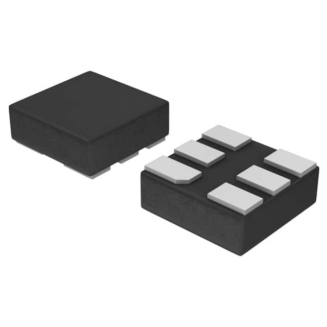
- Package: SOT-353 (SC-88A)
- Essence: High-Speed Logic Gate
- Packaging/Quantity: Tape and Reel, 3000 pieces per reel
Specifications
- Supply Voltage Range: 1.65V to 5.5V
- Input Voltage Range: 0V to VCC
- Output Voltage Range: 0V to VCC
- Operating Temperature Range: -40°C to +85°C
- Propagation Delay Time: 3.2ns (typical)
- Maximum Quiescent Current: 1μA (at 5.5V)
Detailed Pin Configuration
The NLX1G97CMX1TCG has a total of 5 pins: 1. Pin 1: A (Input) 2. Pin 2: B (Input) 3. Pin 3: Y (Output) 4. Pin 4: GND (Ground) 5. Pin 5: VCC (Power Supply)
Functional Features
- Single 2-input NOR gate
- High-speed operation
- Low power consumption
- Wide supply voltage range
- Compatible with TTL and CMOS logic levels
- Schmitt-trigger input for noise immunity
Advantages and Disadvantages
Advantages: - High-speed performance enables quick signal processing. - Low power consumption makes it suitable for battery-powered devices. - Wide supply voltage range allows flexibility in various applications. - Compatibility with TTL and CMOS logic levels simplifies integration into existing systems. - Schmitt-trigger input provides noise immunity, ensuring reliable operation.
Disadvantages: - Limited number of inputs (only 2) restricts complex logic operations. - Small package size may require careful handling during assembly.
Working Principles
The NLX1G97CMX1TCG is a single 2-input NOR gate that operates using CMOS technology. It performs logical NOR operation on the two input signals (A and B) and provides the result at the output pin (Y). The gate operates within a wide supply voltage range, allowing it to function in various voltage environments. Its high-speed performance and low power consumption make it suitable for applications requiring quick signal processing and energy efficiency.
Detailed Application Field Plans
The NLX1G97CMX1TCG can be used in a wide range of applications, including: 1. Digital electronics: Used in digital circuits for logical NOR operations. 2. Microcontrollers: Integrated into microcontroller designs for signal processing. 3. Communication systems: Employed in communication devices for data manipulation. 4. Industrial automation: Utilized in control systems for logical operations. 5. Consumer electronics: Incorporated into various consumer electronic devices for logic functions.
Detailed and Complete Alternative Models
- SN74LVC1G97DBVR - Single 2-Input NOR Gate, SOT-23 Package
- MC74VHC1G02DTT1G - Single 2-Input NOR Gate, SOT-363 Package
- CD4001BM96 - Quad 2-Input NOR Gate, SOIC-14 Package
- 74HCT27PW - Triple 3-Input NOR Gate, TSSOP-14 Package
- HEF4001BT - Quad 2-Input NOR Gate, SOIC-14 Package
These alternative models offer similar functionality and can be considered as substitutes for the NLX1G97CMX1TCG in different applications.
In conclusion, the NLX1G97CMX1TCG is a high-speed logic gate integrated circuit that performs logical NOR operations. Its compact size, low power consumption, and wide supply voltage range make it suitable for various digital applications. However, its limited number of inputs and small package size should be considered when selecting alternative models.
Lista 10 Vanliga frågor och svar relaterade till tillämpningen av NLX1G97CMX1TCG i tekniska lösningar
Sure! Here are 10 common questions and answers related to the application of NLX1G97CMX1TCG in technical solutions:
Q1: What is NLX1G97CMX1TCG? A1: NLX1G97CMX1TCG is a specific integrated circuit (IC) chip that belongs to the family of logic gates. It is commonly used in digital electronics for various technical applications.
Q2: What is the purpose of NLX1G97CMX1TCG? A2: The purpose of NLX1G97CMX1TCG is to perform logical operations, specifically acting as a 2-input multiplexer with an output enable function.
Q3: How does NLX1G97CMX1TCG work? A3: NLX1G97CMX1TCG works by selecting one of two input signals based on the control signal provided. It routes the selected input to the output pin while disabling the other input.
Q4: What are the voltage requirements for NLX1G97CMX1TCG? A4: NLX1G97CMX1TCG typically operates at a supply voltage range of 1.65V to 5.5V.
Q5: Can NLX1G97CMX1TCG be used in battery-powered devices? A5: Yes, NLX1G97CMX1TCG can be used in battery-powered devices as it has a low power consumption and operates within a wide voltage range.
Q6: What are some typical applications of NLX1G97CMX1TCG? A6: NLX1G97CMX1TCG is commonly used in data multiplexing, signal routing, address decoding, and general-purpose switching applications.
Q7: Can NLX1G97CMX1TCG be used in high-speed applications? A7: Yes, NLX1G97CMX1TCG has a fast propagation delay and can be used in high-speed applications where quick switching is required.
Q8: Is NLX1G97CMX1TCG compatible with other logic families? A8: Yes, NLX1G97CMX1TCG is compatible with various logic families such as CMOS, TTL, and LVCMOS.
Q9: What is the package type of NLX1G97CMX1TCG? A9: NLX1G97CMX1TCG is available in a small outline integrated circuit (SOIC) package.
Q10: Where can I find more information about NLX1G97CMX1TCG? A10: You can refer to the datasheet provided by the manufacturer or visit their official website for detailed information on NLX1G97CMX1TCG's specifications, pin configuration, and application notes.
Please note that the answers provided here are general and may vary depending on the specific requirements and use cases.