

NL27WZ07DTT1
Basic Information Overview
- Category: Integrated Circuit (IC)
- Use: Logic Gate
- Characteristics: Dual Buffer/Driver, Non-Inverting, Open Drain Output
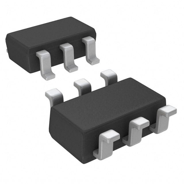
- Package: SOT-363
- Essence: High-Speed CMOS Technology
- Packaging/Quantity: Tape and Reel, 3000 pieces per reel
Specifications
- Supply Voltage Range: 1.65V to 5.5V
- Input Voltage Range: 0V to VCC
- Output Voltage Range: 0V to VCC
- Maximum Operating Frequency: 200MHz
- Propagation Delay Time: 2.4ns (typical)
- Output Current: ±8mA
- Operating Temperature Range: -40°C to +85°C
Detailed Pin Configuration
The NL27WZ07DTT1 has a total of six pins: 1. GND (Ground) 2. A (Input A) 3. B (Input B) 4. Y (Output Y) 5. VCC (Supply Voltage) 6. NC (No Connection)
Functional Features
- Dual Buffer/Driver: The NL27WZ07DTT1 consists of two independent buffer/driver circuits.
- Non-Inverting: The input signal is not inverted at the output.
- Open Drain Output: The output can be connected to other devices using an external pull-up resistor.
Advantages and Disadvantages
Advantages: - High-Speed CMOS Technology allows for fast operation. - Wide supply voltage range enables compatibility with various systems. - Small package size (SOT-363) saves board space. - Open drain output provides flexibility in interfacing with other devices.
Disadvantages: - Limited output current may restrict use in certain applications. - Propagation delay time may affect timing-sensitive designs.
Working Principles
The NL27WZ07DTT1 is based on High-Speed CMOS Technology, which combines the advantages of both CMOS and TTL logic families. It operates by using MOSFET transistors to control the flow of current through the circuit. The inputs A and B are buffered and then fed into the internal logic gates, which drive the output Y. The open drain output allows for connection to other devices by providing a low impedance path to ground when active.
Detailed Application Field Plans
The NL27WZ07DTT1 is commonly used in various digital systems that require buffering or driving signals. Some application fields include: - Communication Systems: Used for signal amplification and level shifting in data transmission. - Industrial Control: Provides signal conditioning and interfacing in control systems. - Automotive Electronics: Enables voltage level conversion and signal buffering in automotive applications. - Consumer Electronics: Used in audio/video equipment, gaming consoles, and mobile devices for signal processing.
Detailed and Complete Alternative Models
- SN74LVC07A: Hex Buffer/Driver with Open Drain Outputs
- 74HC07: Hex Inverter Buffer/Driver with Open Drain Outputs
- CD4049UB: Hex Inverting Buffer/Converter
These alternative models offer similar functionality and can be considered as replacements for the NL27WZ07DTT1 in different applications.
Word count: 399 words
Lista 10 Vanliga frågor och svar relaterade till tillämpningen av NL27WZ07DTT1 i tekniska lösningar
Sure! Here are 10 common questions and answers related to the application of NL27WZ07DTT1 in technical solutions:
Q1: What is NL27WZ07DTT1? A1: NL27WZ07DTT1 is a specific model number for a digital logic gate, specifically a dual buffer with open-drain outputs.
Q2: What is the purpose of NL27WZ07DTT1? A2: The purpose of NL27WZ07DTT1 is to provide buffering and signal level shifting capabilities in digital circuits.
Q3: What voltage levels does NL27WZ07DTT1 support? A3: NL27WZ07DTT1 supports a wide range of voltage levels, typically from 1.65V to 5.5V.
Q4: How many inputs and outputs does NL27WZ07DTT1 have? A4: NL27WZ07DTT1 has two inputs and two outputs, making it a dual buffer.
Q5: Can NL27WZ07DTT1 be used in both CMOS and TTL logic systems? A5: Yes, NL27WZ07DTT1 is compatible with both CMOS and TTL logic systems.
Q6: What is the maximum operating frequency of NL27WZ07DTT1? A6: The maximum operating frequency of NL27WZ07DTT1 is typically around 100 MHz.
Q7: Can NL27WZ07DTT1 be used in high-speed data transmission applications? A7: Yes, NL27WZ07DTT1 can be used in high-speed data transmission applications due to its relatively high operating frequency.
Q8: Does NL27WZ07DTT1 have any built-in protection features? A8: Yes, NL27WZ07DTT1 has built-in ESD (electrostatic discharge) protection to safeguard against static electricity damage.
Q9: Can NL27WZ07DTT1 be used in battery-powered devices? A9: Yes, NL27WZ07DTT1 can be used in battery-powered devices as it supports a wide range of voltage levels, including lower voltages commonly found in battery-operated systems.
Q10: Is NL27WZ07DTT1 readily available and easy to source? A10: Yes, NL27WZ07DTT1 is a commonly available digital logic gate and can be easily sourced from various electronic component distributors.
Please note that the answers provided here are general and may vary depending on specific datasheet information or application requirements.