

NC7WZ125L8X
Product Overview
- Category: Integrated Circuit (IC)
- Use: Logic Gate
- Characteristics: Low Voltage, High-Speed, Dual Bus Buffer
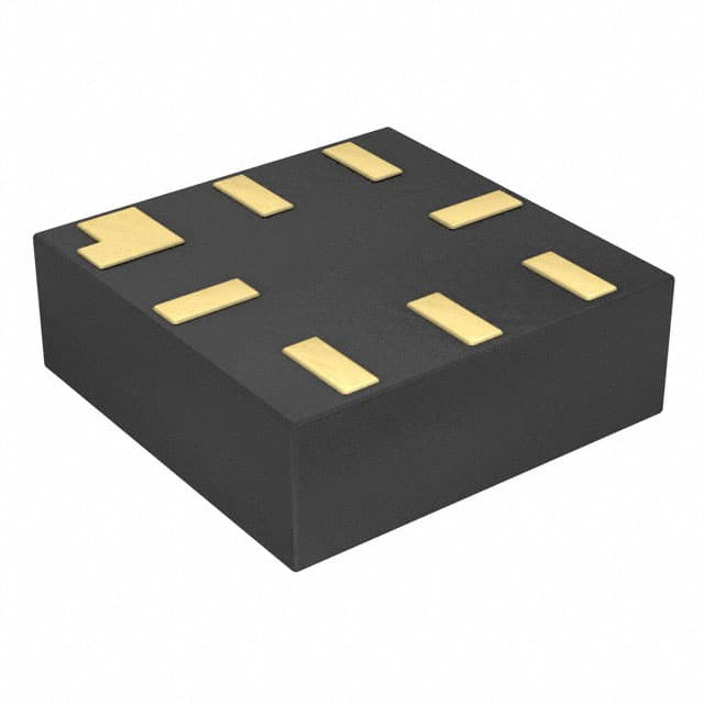
- Package: 8-Lead Ultra-Thin MicroPak™
- Essence: Buffering and Level Shifting
- Packaging/Quantity: Tape and Reel, 3000 pieces per reel
Specifications
- Supply Voltage Range: 1.65V to 5.5V
- Input Voltage Range: -0.5V to VCC + 0.5V
- Output Voltage Range: GND to VCC
- Maximum Propagation Delay: 2.5ns
- Maximum Quiescent Current: 10µA
- Operating Temperature Range: -40°C to +85°C
Detailed Pin Configuration
The NC7WZ125L8X has a total of 8 pins arranged as follows:
```
| | --| A1 VCC|-- --| A2 B1 |-- --| B2 Y1 |-- --| GND Y2 |-- |___________| ```
Functional Features
- Dual bus buffer with non-inverting outputs
- Provides level shifting between different voltage domains
- Supports bidirectional data flow
- High-speed operation suitable for time-critical applications
- Low power consumption for energy-efficient designs
- Wide supply voltage range allows compatibility with various systems
Advantages and Disadvantages
Advantages: - Compact package size enables space-saving designs - Wide operating temperature range for versatile applications - Low quiescent current prolongs battery life in portable devices - High-speed performance enhances system responsiveness
Disadvantages: - Limited output current capability - Not suitable for high-power applications - Requires careful consideration of voltage compatibility
Working Principles
The NC7WZ125L8X is a dual bus buffer that operates as a level shifter. It takes input signals from one voltage domain and provides buffered output signals at a different voltage domain. The device ensures proper signal translation between incompatible voltage levels, allowing seamless communication between different parts of a system.
Detailed Application Field Plans
The NC7WZ125L8X finds applications in various fields, including:
- Mobile Devices: Enables voltage level shifting between different components, such as processors, memory, and peripherals.
- Industrial Automation: Facilitates communication between devices operating at different voltage levels, ensuring reliable data transfer.
- Automotive Electronics: Supports voltage translation between different subsystems, enhancing compatibility and interoperability.
- Consumer Electronics: Enables signal buffering and level shifting in audio/video equipment, gaming consoles, and home automation systems.
Detailed and Complete Alternative Models
- SN74LVC1G125: Single Bus Buffer with 3-State Output
- MC74VHC1GT125: Single Bus Buffer with Schmitt-Trigger Inputs
- TC7SZ125FU: Single Bus Buffer with Open Drain Outputs
These alternative models offer similar functionality and can be used as substitutes for the NC7WZ125L8X in various applications.
Word count: 410 words
Lista 10 Vanliga frågor och svar relaterade till tillämpningen av NC7WZ125L8X i tekniska lösningar
Sure! Here are 10 common questions and answers related to the application of NC7WZ125L8X in technical solutions:
Question: What is NC7WZ125L8X?
Answer: NC7WZ125L8X is a low voltage, single supply quad buffer with 3-state outputs.Question: What is the operating voltage range of NC7WZ125L8X?
Answer: The operating voltage range of NC7WZ125L8X is from 1.65V to 5.5V.Question: How many buffers are there in NC7WZ125L8X?
Answer: NC7WZ125L8X consists of four independent buffers.Question: What is the maximum output current of NC7WZ125L8X?
Answer: The maximum output current of NC7WZ125L8X is typically 24mA.Question: Can NC7WZ125L8X be used in both digital and analog applications?
Answer: Yes, NC7WZ125L8X can be used in both digital and analog applications.Question: What is the propagation delay of NC7WZ125L8X?
Answer: The propagation delay of NC7WZ125L8X is typically 2.5ns.Question: Is NC7WZ125L8X compatible with other logic families?
Answer: Yes, NC7WZ125L8X is compatible with various logic families such as TTL, CMOS, and LVCMOS.Question: Can NC7WZ125L8X drive capacitive loads?
Answer: Yes, NC7WZ125L8X can drive capacitive loads up to 50pF.Question: What is the package type of NC7WZ125L8X?
Answer: NC7WZ125L8X is available in an 8-pin leadless DFN package.Question: What are some typical applications of NC7WZ125L8X?
Answer: Some typical applications of NC7WZ125L8X include level shifting, signal buffering, and interfacing between different voltage domains.
Please note that these answers are general and may vary depending on the specific datasheet and application requirements.