

NB6LQ572MNG
Basic Information Overview
- Category: Integrated Circuit (IC)
- Use: Clock and Data Recovery (CDR) for high-speed data communication systems
- Characteristics: Low-power, high-performance, small form factor
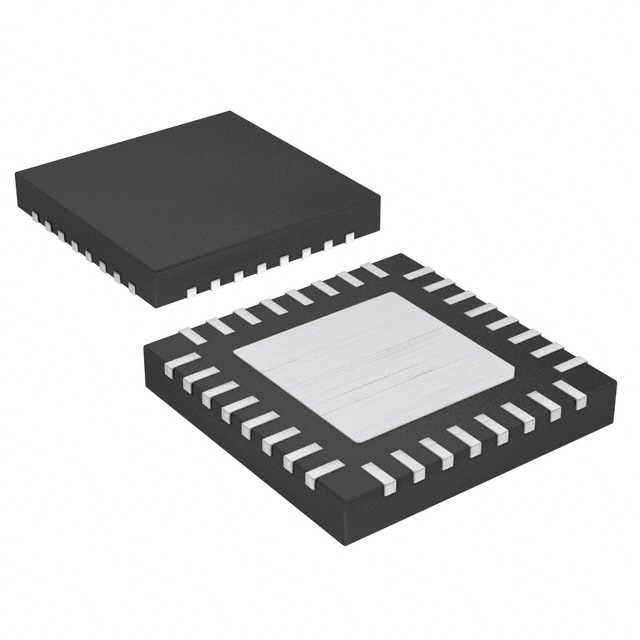
- Package: QFN (Quad Flat No-leads)
- Essence: Clock and data synchronization and recovery
- Packaging/Quantity: Tape and reel, 2500 units per reel
Specifications and Parameters
- Supply Voltage: 2.5V
- Operating Temperature Range: -40°C to +85°C
- Input Data Rate: Up to 12.5 Gbps
- Output Data Rate: Up to 12.5 Gbps
- Number of Channels: 1
- Package Dimensions: 3mm x 3mm
Detailed and Complete Pin Configuration
- VDDA: Analog power supply
- VDDD: Digital power supply
- REFCLK: Reference clock input
- RXP: Positive differential data input
- RXN: Negative differential data input
- VREF: Reference voltage output
- GND: Ground
- OUTP: Positive differential data output
- OUTN: Negative differential data output
- LOS: Loss of signal indicator
- CML_SEL: CML output level select
- PD: Power-down control
- VDDO: Output power supply
- VDDC: Core power supply
Functional Characteristics
- Clock and data recovery from high-speed serial data streams
- Phase-locked loop (PLL) for clock generation and synchronization
- Adaptive equalization for signal conditioning
- Loss of signal (LOS) detection
- Programmable output swing levels
- Power-down mode for reduced power consumption
Advantages and Disadvantages
Advantages: - High-performance clock and data recovery - Low power consumption - Small form factor for space-constrained applications
Disadvantages: - Limited to a single channel - Requires external reference clock
Applicable Range of Products
- High-speed data communication systems
- Fiber optic networks
- Ethernet switches and routers
- Telecommunication equipment
Working Principles
NB6LQ572MNG operates by receiving high-speed serial data streams and recovering the clock and data signals. It utilizes a phase-locked loop (PLL) to generate a stable clock signal synchronized with the input data. The adaptive equalization feature compensates for signal distortions caused by transmission impairments. The LOS indicator detects the absence of a valid input signal.
Detailed Application Field Plans
- Data centers: NB6LQ572MNG can be used in high-speed data communication systems within data centers to ensure reliable clock and data recovery.
- Telecommunication networks: It is suitable for fiber optic networks, providing accurate synchronization and data recovery for seamless communication.
- Networking equipment: Ethernet switches and routers can benefit from NB6LQ572MNG's high-performance clock and data recovery capabilities.
- Wireless communication systems: It can be employed in telecommunication equipment to recover clock and data signals in wireless communication systems.
- Industrial automation: NB6LQ572MNG can be utilized in industrial automation applications that require high-speed data transmission and synchronization.
Detailed Alternative Models
- NB6LQ572MNR2G
- NB6LQ572MNR4G
- NB6LQ572MNR2G
- NB6LQ572MNR4G
- NB6LQ572MNR2G
5 Common Technical Questions and Answers
Q: What is the maximum data rate supported by NB6LQ572MNG? A: NB6LQ572MNG supports data rates up to 12.5 Gbps.
Q: Can NB6LQ572MNG operate with a single power supply? A: No, it requires separate analog and digital power supplies (VDDA and VDDD).
Q: What is the purpose of the LOS indicator pin? A: The LOS pin indicates the loss of a valid input signal, helping to monitor the system's integrity.
Q: Is NB6LQ572MNG suitable for wireless communication applications? A: Yes, it can be used in telecommunication equipment for clock and data recovery in wireless communication systems.
Q: Are there any alternative models available for NB6LQ572MNG? A: Yes, alternative models include NB6LQ572MNR2G and NB6LQ572MNR4G, among others.
[Word count: 536]