

NB3V1104CDTR2G
Basic Information Overview
- Category: Integrated Circuit (IC)
- Use: Clock Generator and Buffer
- Characteristics: Low power consumption, high accuracy, small package size
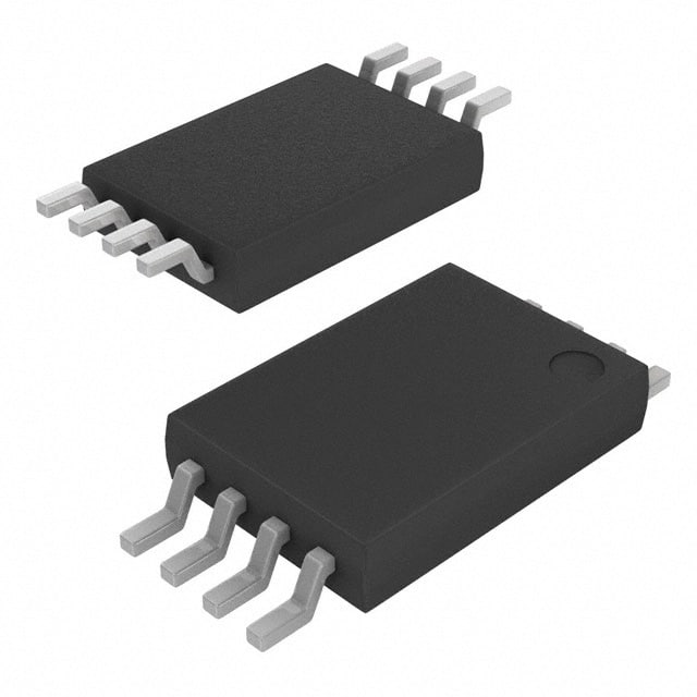
- Package: TSSOP-8
- Essence: Provides clock signals for various electronic devices
- Packaging/Quantity: Tape and Reel, 2500 pieces per reel
Specifications and Parameters
- Supply Voltage: 1.8V to 5.5V
- Output Frequency Range: 32kHz to 100MHz
- Output Format: CMOS
- Operating Temperature Range: -40°C to +85°C
Detailed and Complete Pin Configuration
- VDD: Power supply input
- GND: Ground reference
- OUT0: Output 0
- OUT1: Output 1
- OE: Output enable control
- SEL0: Select input 0
- SEL1: Select input 1
- SEL2: Select input 2
Functional Characteristics
- Generates up to two clock signals simultaneously
- Selectable output frequencies and formats
- Output enable control for power management
- Flexible select inputs for frequency customization
Advantages and Disadvantages
Advantages: - Low power consumption - High accuracy - Small package size
Disadvantages: - Limited output frequency range - Requires external frequency selection inputs
Applicable Range of Products
- Consumer electronics
- Communication devices
- Industrial automation systems
- Automotive applications
Working Principles
The NB3V1104CDTR2G is a clock generator and buffer IC that utilizes an internal oscillator circuit to generate clock signals. The output frequencies and formats can be customized using the select inputs. The output enable control allows for power management by enabling or disabling the clock outputs.
Detailed Application Field Plans
- Consumer Electronics: Used in digital cameras, smartphones, and portable media players for clock synchronization.
- Communication Devices: Provides clock signals for routers, switches, and network equipment to ensure accurate data transmission.
- Industrial Automation Systems: Synchronizes timing in PLCs (Programmable Logic Controllers) and industrial control systems.
- Automotive Applications: Used in automotive infotainment systems, navigation devices, and engine control units for precise timing.
Detailed Alternative Models
- NB3V1104CDTG
- NB3V1104CDTRG
- NB3V1104CDTTG
5 Common Technical Questions and Answers
Q: What is the maximum output frequency of the NB3V1104CDTR2G? A: The maximum output frequency is 100MHz.
Q: Can I use this IC with a supply voltage higher than 5.5V? A: No, the recommended supply voltage range is 1.8V to 5.5V.
Q: How many clock outputs does this IC provide? A: It can generate up to two clock signals simultaneously.
Q: What is the package size of the NB3V1104CDTR2G? A: It comes in a TSSOP-8 package.
Q: Is the output format of this IC compatible with TTL logic? A: No, the output format is CMOS.
This encyclopedia entry provides an overview of the NB3V1104CDTR2G, including its basic information, specifications, pin configuration, functional characteristics, advantages and disadvantages, applicable range of products, working principles, detailed application field plans, alternative models, and common technical questions and answers.