

NB3N15625MNTXG
Product Overview
- Category: Integrated Circuit
- Use: Clock Generator and Multiplier
- Characteristics: High-performance, low-jitter, low-power consumption
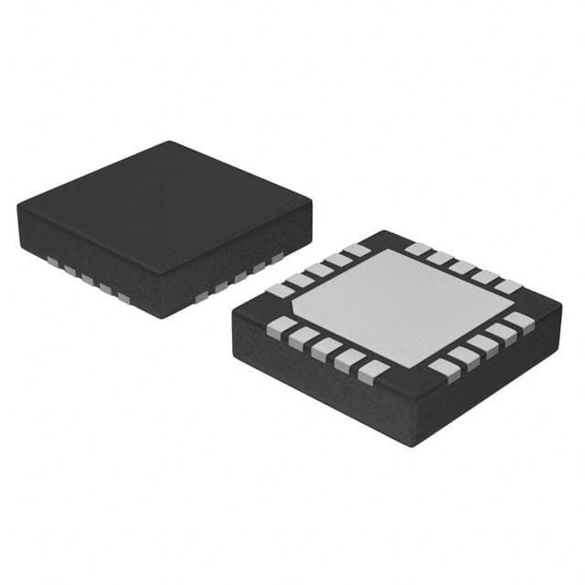
- Package: Surface Mount Technology (SMT)
- Essence: Clock generation and multiplication for various applications
- Packaging/Quantity: Tape and Reel, 3000 units per reel
Specifications
- Input Voltage: 1.8V to 3.3V
- Output Frequency Range: 10MHz to 200MHz
- Operating Temperature Range: -40°C to +85°C
- Supply Current: 15mA typical
- Output Type: LVCMOS
Detailed Pin Configuration
The NB3N15625MNTXG has a total of 16 pins. The pin configuration is as follows:
- VDD
- GND
- OUT0
- OUT1
- OUT2
- OUT3
- OUT4
- OUT5
- OUT6
- OUT7
- OE#
- SEL0
- SEL1
- SEL2
- SEL3
- SEL4
Functional Features
- Generates multiple clock outputs from a single input frequency
- Provides selectable output frequencies through SEL pins
- Low jitter and phase noise for high-quality clock signals
- Wide operating voltage range for compatibility with various systems
- Power-saving design with low supply current
Advantages and Disadvantages
Advantages: - Versatile clock generation and multiplication capabilities - High-performance output signals with low jitter - Wide operating voltage range for flexibility - Power-efficient design for reduced energy consumption
Disadvantages: - Limited output frequency range compared to some specialized clock generators - Requires careful selection of SEL pins for desired output frequency
Working Principles
The NB3N15625MNTXG is a clock generator and multiplier integrated circuit. It takes an input frequency and generates multiple clock outputs with selectable frequencies. The output frequencies can be set using the SEL pins, allowing flexibility in various applications.
The device operates by dividing the input frequency using a phase-locked loop (PLL) and then multiplying it to achieve the desired output frequency. This process ensures accurate and stable clock signals with low jitter and phase noise.
Detailed Application Field Plans
The NB3N15625MNTXG finds applications in various fields where precise clock generation and multiplication are required. Some potential application areas include:
- Telecommunications: Clock synchronization in network equipment and communication systems.
- Data Centers: Timing control for servers, switches, and storage devices.
- Consumer Electronics: Clock generation for audio/video equipment, gaming consoles, and smart home devices.
- Industrial Automation: Timing control in industrial machinery, robotics, and control systems.
- Automotive: Clock synchronization in automotive electronics, infotainment systems, and driver assistance systems.
Detailed and Complete Alternative Models
- NB3N502DG: Clock Generator and Multiplier with wider output frequency range.
- NB3N3001DTG: Programmable Clock Generator with additional features such as frequency synthesis and spread spectrum modulation.
- NB3N2304DTG: Low-Jitter Clock Generator with differential output capability.
These alternative models offer different specifications and features to cater to specific application requirements.
Word count: 345 words
Lista 10 Vanliga frågor och svar relaterade till tillämpningen av NB3N15625MNTXG i tekniska lösningar
Sure! Here are 10 common questions and answers related to the application of NB3N15625MNTXG in technical solutions:
Q: What is NB3N15625MNTXG? A: NB3N15625MNTXG is a specific model number for a clock generator IC (integrated circuit) manufactured by ON Semiconductor.
Q: What is the purpose of NB3N15625MNTXG? A: The purpose of NB3N15625MNTXG is to generate clock signals with precise frequencies and timings, which are essential for synchronizing various components in electronic systems.
Q: What are the key features of NB3N15625MNTXG? A: Some key features of NB3N15625MNTXG include low jitter, wide frequency range, multiple outputs, programmable dividers, and compatibility with different voltage levels.
Q: In what applications can NB3N15625MNTXG be used? A: NB3N15625MNTXG can be used in various applications such as telecommunications, networking equipment, data centers, industrial automation, and high-speed digital systems.
Q: How does NB3N15625MNTXG help in system synchronization? A: NB3N15625MNTXG generates clock signals that synchronize different components, ensuring proper timing and coordination between them, which is crucial for reliable system operation.
Q: Can NB3N15625MNTXG generate multiple clock frequencies simultaneously? A: Yes, NB3N15625MNTXG has multiple output channels that can generate different clock frequencies simultaneously, allowing for flexible system design.
Q: Is NB3N15625MNTXG programmable? A: Yes, NB3N15625MNTXG is programmable, meaning its parameters such as frequency, phase, and output format can be configured using control inputs or software.
Q: What is the typical power supply voltage for NB3N15625MNTXG? A: The typical power supply voltage for NB3N15625MNTXG is in the range of 2.5V to 3.3V, making it compatible with common digital logic levels.
Q: Does NB3N15625MNTXG support external clock inputs? A: Yes, NB3N15625MNTXG supports external clock inputs, allowing it to synchronize with an external reference signal if required.
Q: Are evaluation boards or application notes available for NB3N15625MNTXG? A: Yes, ON Semiconductor provides evaluation boards and application notes that help users understand and implement NB3N15625MNTXG in their technical solutions.
Please note that the specific details and answers may vary depending on the manufacturer's documentation and the application requirements.