

NB3F8L3010CMNG
Basic Information Overview
- Category: Electronic Component
- Use: Signal Amplification and Switching
- Characteristics: High Gain, Low Noise, Fast Switching Speed
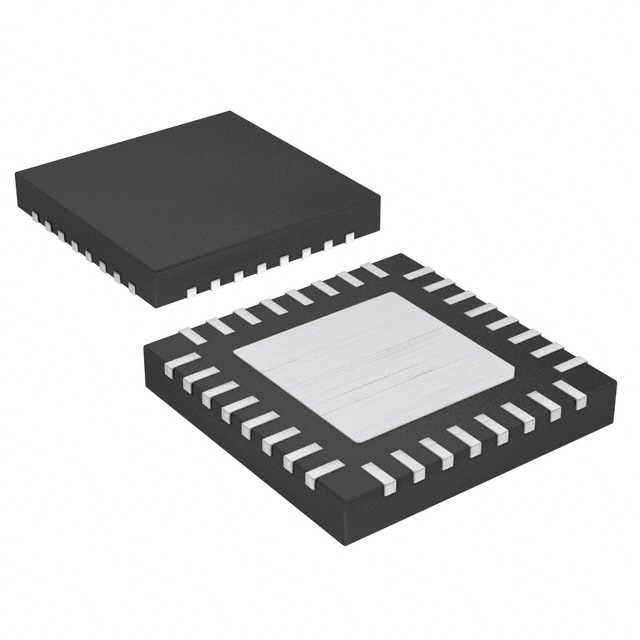
- Package: SMD (Surface Mount Device)
- Essence: NPN Bipolar Junction Transistor
- Packaging/Quantity: Tape and Reel, 3000 pieces per reel
Specifications and Parameters
- Collector Current (IC): 100mA
- Collector-Emitter Voltage (VCEO): 30V
- Emitter-Base Voltage (VEBO): 5V
- Power Dissipation (PD): 200mW
- Transition Frequency (fT): 250MHz
- Operating Temperature Range: -55°C to +150°C
Detailed and Complete Pin Configuration
- Base (B)
- Emitter (E)
- Collector (C)
Functional Characteristics
- High current gain (hFE)
- Low noise figure
- Fast switching speed
- Suitable for low-power applications
- Wide operating temperature range
Advantages and Disadvantages
Advantages: - High gain allows for signal amplification - Low noise figure ensures minimal distortion - Fast switching speed enables rapid switching between states - Suitable for low-power applications, conserving energy - Wide operating temperature range allows for versatile use
Disadvantages: - Limited maximum collector current (100mA) - Restricted maximum collector-emitter voltage (30V) - Relatively low power dissipation capability (200mW)
Applicable Range of Products
- Audio Amplifiers
- RF Amplifiers
- Switching Circuits
- Oscillators
- Logic Gates
Working Principles
The NB3F8L3010CMNG is an NPN bipolar junction transistor. It consists of three layers of semiconductor material, namely the emitter, base, and collector. When a small current flows into the base terminal, it controls a larger current flowing between the collector and emitter terminals. This allows for signal amplification and switching.
Detailed Application Field Plans
- Audio Amplifiers: The transistor can be used to amplify weak audio signals, enhancing sound quality.
- RF Amplifiers: It is suitable for amplifying radio frequency signals in communication systems.
- Switching Circuits: The fast switching speed makes it ideal for digital switching applications.
- Oscillators: The transistor can be utilized in oscillator circuits to generate stable oscillations.
- Logic Gates: It can be incorporated into logic gate circuits for digital signal processing.
Detailed Alternative Models
- NB3F8L3010CMN
- NB3F8L3010CNG
- NB3F8L3010CMNP
- NB3F8L3010CMNPG
5 Common Technical Questions and Answers
Q: What is the maximum collector current of NB3F8L3010CMNG? A: The maximum collector current is 100mA.
Q: What is the operating temperature range of this transistor? A: The operating temperature range is -55°C to +150°C.
Q: Can NB3F8L3010CMNG be used in high-power applications? A: No, it is more suitable for low-power applications due to its limited power dissipation capability.
Q: What is the purpose of the base terminal in this transistor? A: The base terminal controls the flow of current between the collector and emitter terminals, allowing for signal amplification and switching.
Q: Is NB3F8L3010CMNG compatible with logic gate circuits? A: Yes, it can be integrated into logic gate circuits for digital signal processing.