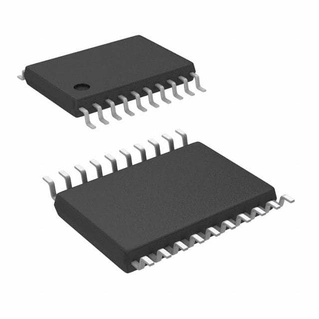
MC74LCX541DTR2
Product Overview
- Category: Integrated Circuit (IC)
- Use: Logic Level Shifter
- Characteristics: High-speed, low-voltage, octal buffer/line driver
- Package: TSSOP-20
- Essence: This IC is designed to shift logic levels between different voltage domains, allowing seamless communication between devices operating at different voltage levels.
- Packaging/Quantity: Available in tape and reel packaging, with 2500 units per reel.
Specifications
- Supply Voltage: 1.65V to 5.5V
- Logic Family: LCX
- Number of Channels: 8
- Input/Output Compatibility: TTL, CMOS
- Propagation Delay: 3.5ns (typical)
- Output Drive Capability: ±24mA
- Operating Temperature Range: -40°C to +85°C
Pin Configuration
The MC74LCX541DTR2 has a TSSOP-20 package with the following pin configuration:
┌───┬───┐
   OE ─┤1  20├ VCC
  A1Y ─┤2  19├ A2Y
  A1A ─┤3  18├ A2A
  GND ─┤4  17├ A2
  A1B ─┤5  16├ A2B
  A1 ──┤6  15├ A2Y
  Y1 ──┤7  14├ Y2
  Y1A ─┤8  13├ Y2A
  Y1B ─┤9  12├ Y2B
  GND ─┤10 11├ Y2Y
       └───┴───┘
Functional Features
- High-speed operation: The MC74LCX541DTR2 offers fast propagation delay, allowing for efficient data transmission.
- Wide supply voltage range: It can operate within a wide voltage range from 1.65V to 5.5V, making it compatible with various systems.
- Octal buffer/line driver: The IC provides eight channels of buffering and line driving capability, enabling bidirectional communication between different voltage domains.
- Output drive capability: With a ±24mA output drive capability, it can easily drive capacitive loads and long traces.
Advantages and Disadvantages
Advantages: - Fast propagation delay ensures quick data transmission. - Wide supply voltage range allows compatibility with various systems. - Bidirectional communication between different voltage domains. - Can drive capacitive loads and long traces effectively.
Disadvantages: - Limited number of channels (8) may not be sufficient for complex systems requiring more connections. - TSSOP package may require careful handling during assembly.
Working Principles
The MC74LCX541DTR2 is a logic level shifter that operates by translating signals between different voltage levels. It utilizes a combination of CMOS and TTL logic families to achieve bidirectional communication. The input signals are shifted to the desired voltage level and then buffered to provide reliable outputs. The IC's high-speed operation ensures minimal delay in signal transmission.
Detailed Application Field Plans
The MC74LCX541DTR2 finds applications in various fields where logic level shifting is required. Some potential application areas include:
- Microcontroller Interfacing: It can be used to interface microcontrollers operating at different voltage levels, enabling seamless communication between them.
- Mixed Voltage Systems: In systems with mixed voltage domains, the IC can facilitate communication between different components operating at varying voltage levels.
- Data Communication: It can be employed in data communication systems to ensure compatibility between devices operating at different logic levels.
- Sensor Networks: The IC can be utilized in sensor networks where sensors operate at different voltage levels, allowing efficient data exchange.
Detailed and Complete Alternative Models
- SN74LVC541A: This octal buffer/line driver offers similar functionality and is available in various package options.
- 74HC541: A popular alternative, this IC provides eight buffer/line driver channels and operates at a higher voltage range.
- CD74HCT541: This IC is compatible with TTL logic levels and offers eight buffer/line driver channels.
These alternative models provide similar logic level shifting capabilities and can be considered based on specific requirements and availability.
Word count: 511 words
Lista 10 Vanliga frågor och svar relaterade till tillämpningen av MC74LCX541DTR2 i tekniska lösningar
Sure! Here are 10 common questions and answers related to the application of MC74LCX541DTR2 in technical solutions:
Q: What is MC74LCX541DTR2? A: MC74LCX541DTR2 is a high-performance, low-voltage, octal buffer with 3-state outputs. It is commonly used for signal buffering and level shifting applications.
Q: What is the operating voltage range of MC74LCX541DTR2? A: The operating voltage range of MC74LCX541DTR2 is typically between 2.0V and 3.6V.
Q: What is the maximum output current of MC74LCX541DTR2? A: The maximum output current of MC74LCX541DTR2 is typically 24mA.
Q: Can MC74LCX541DTR2 be used for bidirectional communication? A: No, MC74LCX541DTR2 is a unidirectional buffer and cannot be used for bidirectional communication.
Q: What is the propagation delay of MC74LCX541DTR2? A: The propagation delay of MC74LCX541DTR2 is typically around 3.5ns.
Q: Can MC74LCX541DTR2 be used in high-speed applications? A: Yes, MC74LCX541DTR2 is designed for high-speed operation and can be used in applications requiring fast signal switching.
Q: Does MC74LCX541DTR2 have internal pull-up or pull-down resistors? A: No, MC74LCX541DTR2 does not have internal pull-up or pull-down resistors. External resistors may be required for proper signal termination.
Q: Can MC74LCX541DTR2 tolerate overvoltage on its inputs? A: No, MC74LCX541DTR2 is not designed to tolerate overvoltage on its inputs. Proper voltage level translation should be implemented if necessary.
Q: What is the maximum operating frequency of MC74LCX541DTR2? A: The maximum operating frequency of MC74LCX541DTR2 is typically around 200MHz.
Q: Is MC74LCX541DTR2 available in different package options? A: Yes, MC74LCX541DTR2 is available in various package options, including SOIC, TSSOP, and PDIP.
Please note that the answers provided here are general and may vary depending on specific datasheet specifications and application requirements.


