

MC10E112FNR2G
Product Overview
- Category: Integrated Circuit (IC)
- Use: Digital Logic Gate
- Characteristics: High-speed, ECL (Emitter-Coupled Logic) Technology
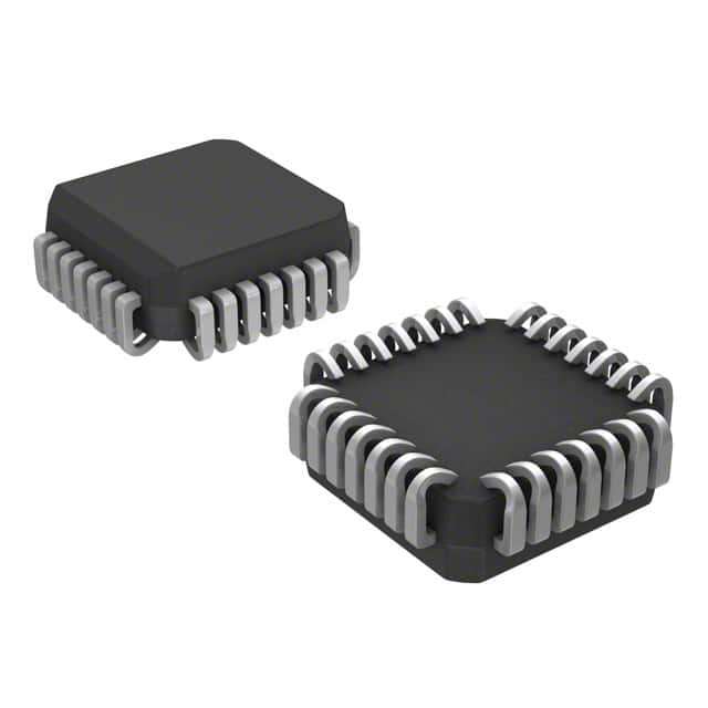
- Package: 28-pin PLCC (Plastic Leaded Chip Carrier)
- Essence: Dual Negative-Edge-Triggered J-K Flip-Flop
- Packaging/Quantity: Tape and Reel, 2500 units per reel
Specifications
- Supply Voltage: -4.2V to -5.7V
- Operating Temperature: -40°C to +85°C
- Propagation Delay: 1.8 ns (typical)
- Output Current: ±24 mA
- Input Voltage: -2.0V to -5.7V
- Output Voltage: -2.0V to -5.7V
Detailed Pin Configuration
The MC10E112FNR2G has a total of 28 pins. The pin configuration is as follows:
- Q1
- K1
- J1
- CLK1
- VEE
- D1
- Q2
- K2
- J2
- CLK2
- GND
- D2
- Q3
- K3
- J3
- CLK3
- VCC
- D3
- Q4
- K4
- J4
- CLK4
- VBB
- D4
- Q5
- K5
- J5
- CLK5
Functional Features
- Dual negative-edge-triggered J-K flip-flop with asynchronous clear
- Operates at high-speed using ECL technology
- Provides reliable and precise digital logic functionality
- Supports synchronous operation with common clock inputs
Advantages and Disadvantages
Advantages
- High-speed operation allows for efficient data processing
- ECL technology provides excellent noise immunity
- Dual flip-flop design enhances flexibility in circuit design
- Asynchronous clear input enables easy reset of the flip-flops
Disadvantages
- Requires a negative power supply, limiting compatibility with some systems
- Higher power consumption compared to CMOS-based logic gates
- Limited availability of alternative models due to specific characteristics
Working Principles
The MC10E112FNR2G is based on ECL technology, which utilizes differential signaling and current-mode logic. The dual negative-edge-triggered J-K flip-flop operates by storing and manipulating binary data. The asynchronous clear input allows for resetting the flip-flops independently of the clock signal.
Detailed Application Field Plans
The MC10E112FNR2G is commonly used in applications that require high-speed digital logic operations. Some potential application fields include:
- Telecommunications: Used in high-speed data transmission systems.
- Networking: Employed in network switches and routers for efficient packet processing.
- Test and Measurement: Utilized in equipment for accurate data acquisition and analysis.
- Industrial Automation: Integrated into control systems for precise timing and synchronization.
- Aerospace and Defense: Applied in radar systems and avionics for reliable signal processing.
Detailed and Complete Alternative Models
While the MC10E112FNR2G has specific characteristics, there are alternative models available that offer similar functionality. Some alternatives to consider are:
- MC100EP116: 6-Bit Differential Receiver/Driver
- MC100ELT23: Differential PECL/TTL Translator
- MC100LVEL56: 2:1 Multiplexer with Differential Outputs
- MC100LVELT23: Differential ECL/TTL Translator
These alternative models provide different features and pin configurations, allowing for flexibility in circuit design based on specific requirements.
Word count: 420 words
Lista 10 Vanliga frågor och svar relaterade till tillämpningen av MC10E112FNR2G i tekniska lösningar
Sure! Here are 10 common questions and answers related to the application of MC10E112FNR2G in technical solutions:
Q: What is MC10E112FNR2G? A: MC10E112FNR2G is a specific model number for a high-speed ECL (Emitter-Coupled Logic) dual JK flip-flop integrated circuit.
Q: What are the key features of MC10E112FNR2G? A: Some key features of MC10E112FNR2G include high-speed operation, differential inputs, and outputs, and compatibility with ECL logic families.
Q: What is the typical operating voltage range for MC10E112FNR2G? A: The typical operating voltage range for MC10E112FNR2G is between -4.2V and -5.7V.
Q: Can MC10E112FNR2G be used in low-power applications? A: No, MC10E112FNR2G is not designed for low-power applications as it operates at higher voltages and consumes more power compared to low-power logic families.
Q: What is the maximum clock frequency supported by MC10E112FNR2G? A: MC10E112FNR2G can support clock frequencies up to several gigahertz, depending on the specific conditions and setup.
Q: How many flip-flops are there in MC10E112FNR2G? A: MC10E112FNR2G contains two independent JK flip-flops.
Q: Can MC10E112FNR2G be cascaded to create larger counters or shift registers? A: Yes, MC10E112FNR2G can be cascaded with other compatible flip-flops to create larger counters or shift registers.
Q: What is the typical propagation delay of MC10E112FNR2G? A: The typical propagation delay of MC10E112FNR2G is in the range of a few nanoseconds.
Q: Is MC10E112FNR2G suitable for high-speed data communication applications? A: Yes, MC10E112FNR2G is commonly used in high-speed data communication applications where precise timing and fast operation are required.
Q: Can MC10E112FNR2G operate in harsh environments? A: MC10E112FNR2G is not specifically designed for harsh environments, so additional precautions may be necessary to ensure reliable operation in such conditions.
Please note that these answers are general and may vary depending on specific application requirements and datasheet specifications.