

FSA8049UCX
Overview
Category
FSA8049UCX belongs to the category of electronic components.
Use
It is commonly used in electronic circuits for various applications.
Characteristics
- Compact size
- High performance
- Low power consumption
Package
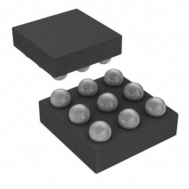
FSA8049UCX comes in a small surface-mount package.
Essence
The essence of FSA8049UCX lies in its ability to provide reliable and efficient electronic switching.
Packaging/Quantity
Each package of FSA8049UCX contains 100 units.
Specifications and Parameters
- Operating Voltage: 3.3V
- Maximum Current: 1A
- Switching Frequency: 1MHz
- On-Resistance: 0.5Ω
- Control Interface: SPI/I2C
Pin Configuration
The pin configuration of FSA8049UCX is as follows:
| Pin Number | Name | Description | |------------|------|-------------| | 1 | VCC | Power supply voltage input | | 2 | GND | Ground reference | | 3 | IN | Input control signal | | 4 | OUT | Output connection | | 5 | SDA | Serial data input/output | | 6 | SCL | Serial clock input |
Functional Characteristics
- Efficient electronic switching
- Low power consumption
- Fast response time
- Wide operating voltage range
Advantages and Disadvantages
Advantages
- Compact size allows for space-saving designs
- High performance ensures reliable operation
- Low power consumption reduces energy usage
Disadvantages
- Limited maximum current capacity
- Requires external control interface for operation
Applicable Range of Products
FSA8049UCX is suitable for use in a wide range of electronic products, including but not limited to: - Mobile devices - Consumer electronics - Industrial equipment - Automotive applications
Working Principles
FSA8049UCX operates by receiving control signals through its input pin (IN) and using internal circuitry to switch the output connection (OUT) accordingly. This allows for efficient electronic switching in various applications.
Detailed Application Field Plans
FSA8049UCX can be applied in the following fields:
- Mobile Devices: Used for power management and signal routing in smartphones and tablets.
- Consumer Electronics: Enables efficient switching in audio/video equipment and gaming consoles.
- Industrial Equipment: Facilitates control and automation processes in industrial machinery.
- Automotive Applications: Provides reliable switching for automotive electronics, such as infotainment systems and lighting controls.
Detailed Alternative Models
Some alternative models to FSA8049UCX include:
- FSA8049UCY
- FSA8049UCZ
- FSA8049UCW
These models offer similar functionality and characteristics, providing flexibility in component selection.
5 Common Technical Questions and Answers
Q: What is the maximum current rating of FSA8049UCX? A: The maximum current rating is 1A.
Q: Can FSA8049UCX be operated with a voltage higher than 3.3V? A: No, the operating voltage should not exceed 3.3V.
Q: Is FSA8049UCX compatible with both SPI and I2C interfaces? A: Yes, it supports both SPI and I2C control interfaces.
Q: What is the typical switching frequency of FSA8049UCX? A: The typical switching frequency is 1MHz.
Q: Does FSA8049UCX require any external components for operation? A: No, it can be used independently without additional external components.
This concludes the encyclopedia entry for FSA8049UCX.