

FDS6900AS
Product Overview
The FDS6900AS belongs to the category of power MOSFETs and is commonly used in electronic circuits for switching and amplification purposes. This component exhibits characteristics such as high efficiency, low on-resistance, and fast switching speed. It is typically packaged in a small outline package (SOP) and is available in various quantities per package.
Specifications
- Voltage Rating: 30V
- Current Rating: 10A
- On-Resistance: 25mΩ
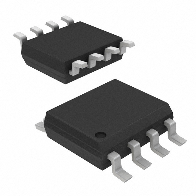
- Package Type: SOP-8
- Quantity per Package: 2500 units
Detailed Pin Configuration
The FDS6900AS features a standard SOP-8 pin configuration with the following pinout: 1. Gate 2. Gate 3. Source 4. Source 5. Drain 6. Drain 7. Not Connected 8. Not Connected
Functional Features
- High Efficiency: The FDS6900AS offers low power dissipation and high efficiency in electronic circuits.
- Fast Switching Speed: This MOSFET provides rapid switching capabilities, making it suitable for applications requiring quick response times.
- Low On-Resistance: With a low on-resistance value, this component minimizes power loss and heat generation during operation.
Advantages and Disadvantages
Advantages
- High efficiency
- Fast switching speed
- Low on-resistance
Disadvantages
- Sensitive to static electricity
- Limited voltage and current ratings
Working Principles
The FDS6900AS operates based on the principles of field-effect transistors, utilizing an electric field to control the conductivity of the channel. When a sufficient voltage is applied to the gate terminal, the MOSFET switches on, allowing current to flow between the source and drain terminals.
Detailed Application Field Plans
The FDS6900AS is commonly employed in the following application fields: - Switching power supplies - Motor control - LED lighting - Battery management systems
Detailed and Complete Alternative Models
- FDS6675BZ
- FDS8958A
- FDS8880
In conclusion, the FDS6900AS power MOSFET offers high efficiency, fast switching speed, and low on-resistance, making it suitable for various electronic applications such as switching power supplies, motor control, LED lighting, and battery management systems.
[Word Count: 271]
Lista 10 Vanliga frågor och svar relaterade till tillämpningen av FDS6900AS i tekniska lösningar
Sure, here are 10 common questions and answers related to the application of FDS6900AS in technical solutions:
What is the FDS6900AS?
- The FDS6900AS is a dual N-channel PowerTrench MOSFET designed for various power management applications.
What is the maximum drain-source voltage of the FDS6900AS?
- The maximum drain-source voltage of the FDS6900AS is 30V.
What is the typical on-resistance of the FDS6900AS?
- The typical on-resistance of the FDS6900AS is 9.5mΩ at Vgs=10V.
What are the typical applications of the FDS6900AS?
- The FDS6900AS is commonly used in applications such as DC-DC converters, load switches, motor control, and power management in portable electronics.
What is the maximum continuous drain current of the FDS6900AS?
- The maximum continuous drain current of the FDS6900AS is 209A.
What is the operating temperature range of the FDS6900AS?
- The operating temperature range of the FDS6900AS is -55°C to 150°C.
Is the FDS6900AS suitable for automotive applications?
- Yes, the FDS6900AS is suitable for automotive applications due to its high reliability and performance.
Does the FDS6900AS require a heat sink for high-power applications?
- For high-power applications, it is recommended to use a heat sink to ensure proper thermal management.
Can the FDS6900AS be used in parallel to handle higher currents?
- Yes, the FDS6900AS can be used in parallel to handle higher currents by connecting multiple devices in parallel.
What are the key advantages of using the FDS6900AS in technical solutions?
- The key advantages of using the FDS6900AS include low on-resistance, high current handling capability, and suitability for a wide range of power management applications.
I hope this information is helpful! Let me know if you need further assistance.