

FDPF33N25T
Introduction
The FDPF33N25T is a power MOSFET belonging to the category of electronic components used in various applications. This entry provides an overview of the basic information, specifications, pin configuration, functional features, advantages and disadvantages, working principles, application field plans, and alternative models of the FDPF33N25T.
Basic Information Overview
- Category: Power MOSFET
- Use: The FDPF33N25T is commonly used as a switching device in power supply circuits, motor control, and other high-power applications.
- Characteristics: It exhibits low on-state resistance, high switching speed, and low gate charge, making it suitable for high-efficiency power conversion.
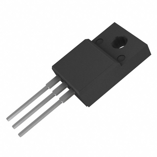
- Package: The FDPF33N25T is typically available in a TO-220F package.
- Essence: It serves as a crucial component in power electronics, enabling efficient power management and control.
- Packaging/Quantity: It is usually packaged in reels or tubes, with varying quantities based on manufacturer specifications.
Specifications
- Voltage Rating: 250V
- Current Rating: 33A
- On-State Resistance: 0.09Ω
- Gate-Source Voltage (Max): ±20V
- Operating Temperature Range: -55°C to 150°C
Detailed Pin Configuration
The FDPF33N25T typically has three pins: 1. Gate (G): Input terminal for controlling the switching operation. 2. Drain (D): Output terminal connected to the load. 3. Source (S): Common terminal and reference point for the input and output circuits.
Functional Features
- High Efficiency: Low on-state resistance and gate charge contribute to high efficiency in power conversion applications.
- Fast Switching: High switching speed enables rapid response in switching operations.
- Reliability: Robust design and thermal performance ensure reliable operation in demanding environments.
Advantages and Disadvantages
Advantages
- High efficiency in power conversion
- Fast switching speed
- Reliable performance in demanding conditions
Disadvantages
- Sensitive to static electricity and voltage spikes
- Requires careful handling and protection in circuit design
Working Principles
The FDPF33N25T operates based on the principle of field-effect transistors, where the voltage applied to the gate terminal controls the flow of current between the drain and source terminals. By modulating the gate voltage, the MOSFET can efficiently switch high-power loads on and off.
Detailed Application Field Plans
The FDPF33N25T finds extensive use in the following applications: - Switching power supplies - Motor control circuits - Inverters and converters - Electronic ballasts - Audio amplifiers
Detailed and Complete Alternative Models
- IRF3205: Similar power MOSFET with comparable specifications.
- STP55NF06L: Alternative MOSFET offering similar performance characteristics.
- IXFH50N60Q: Power MOSFET suitable for high-power applications.
In conclusion, the FDPF33N25T power MOSFET offers high efficiency, fast switching, and reliability, making it a valuable component in various power electronics applications.
[Word Count: 413]
Lista 10 Vanliga frågor och svar relaterade till tillämpningen av FDPF33N25T i tekniska lösningar
What is FDPF33N25T?
- FDPF33N25T is a power MOSFET designed for high-speed switching applications in power supplies, motor control, and other electronic systems.
What is the maximum drain-source voltage of FDPF33N25T?
- The maximum drain-source voltage of FDPF33N25T is 250V.
What is the continuous drain current rating of FDPF33N25T?
- The continuous drain current rating of FDPF33N25T is 33A.
What is the on-resistance of FDPF33N25T?
- The on-resistance of FDPF33N25T is typically 0.08 ohms.
Can FDPF33N25T be used in motor control applications?
- Yes, FDPF33N25T is suitable for motor control applications due to its high-speed switching capability and high current handling capacity.
Is FDPF33N25T suitable for use in power supply designs?
- Yes, FDPF33N25T is commonly used in power supply designs due to its high voltage and current ratings.
What are the typical thermal characteristics of FDPF33N25T?
- FDPF33N25T has a low thermal resistance and is designed to efficiently dissipate heat during operation.
Does FDPF33N25T require a heat sink in high-power applications?
- In high-power applications, it is recommended to use a heat sink with FDPF33N25T to ensure proper thermal management.
What are the common failure modes of FDPF33N25T?
- Common failure modes of FDPF33N25T include overcurrent conditions, overvoltage stress, and excessive temperature leading to thermal breakdown.
Are there any application notes or reference designs available for using FDPF33N25T in technical solutions?
- Yes, several application notes and reference designs are available from the manufacturer to guide engineers in implementing FDPF33N25T in various technical solutions.