

BD538K Product Overview
Introduction
BD538K is a semiconductor product belonging to the category of integrated circuits. It is widely used in electronic devices and offers various characteristics that make it suitable for a range of applications. This entry provides an overview of BD538K, including its basic information, specifications, pin configuration, functional features, advantages and disadvantages, working principles, application field plans, and alternative models.
Basic Information Overview
- Category: Integrated Circuits
- Use: BD538K is utilized in electronic circuitry for amplification and signal processing.
- Characteristics: It exhibits high gain, low noise, and low distortion characteristics, making it suitable for audio and instrumentation applications.
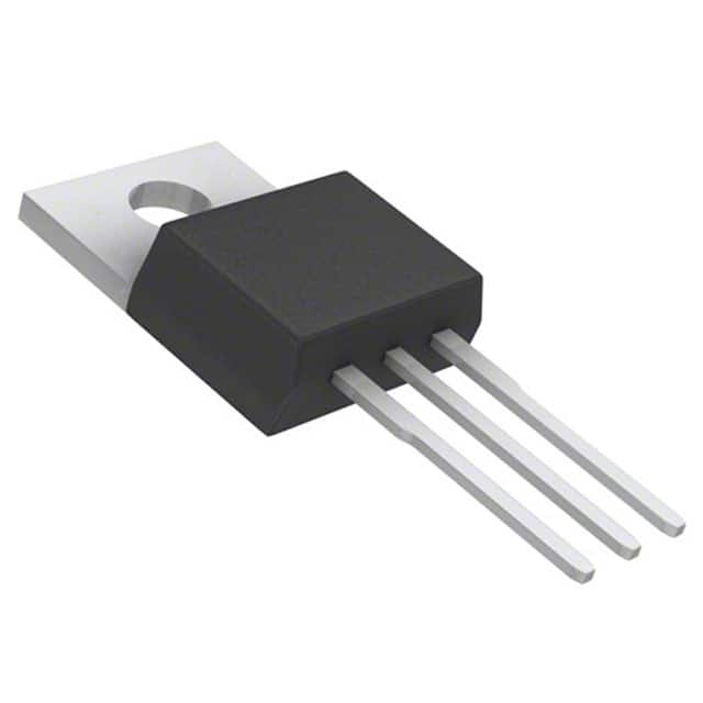
- Package: BD538K is available in a standard TO-220 package.
- Essence: The essence of BD538K lies in its ability to provide reliable amplification and signal processing capabilities.
- Packaging/Quantity: It is typically packaged individually and available in varying quantities based on customer requirements.
Specifications
The specifications of BD538K include: - Maximum Power Dissipation: 2.5W - Collector-Emitter Voltage: 80V - DC Current Gain (hFE): 40 - 250 - Transition Frequency: 30MHz - Operating Temperature Range: -65°C to +150°C
Detailed Pin Configuration
The detailed pin configuration of BD538K is as follows: 1. Base (B) 2. Collector (C) 3. Emitter (E)
Functional Features
BD538K offers the following functional features: - High gain amplification - Low noise operation - Low distortion output
Advantages and Disadvantages
Advantages
- Reliable amplification performance
- Low noise output
- Wide operating temperature range
Disadvantages
- Limited maximum power dissipation
- Moderate transition frequency
Working Principles
BD538K operates based on the principles of bipolar junction transistors, utilizing its three terminals for signal amplification and processing. When biased and connected within a circuit, it facilitates the amplification of input signals with minimal distortion and noise.
Detailed Application Field Plans
BD538K finds extensive application in the following fields: - Audio amplification systems - Instrumentation equipment - Signal processing circuits
Detailed and Complete Alternative Models
Some alternative models to BD538K include: - BC547 - 2N3904 - BC548 - 2N2222
In conclusion, BD538K serves as a crucial component in electronic circuitry, offering reliable amplification and signal processing capabilities across various applications.
Word Count: 330
Lista 10 Vanliga frågor och svar relaterade till tillämpningen av BD538K i tekniska lösningar
What is BD538K?
- BD538K is a high-performance adhesive or sealant commonly used in technical solutions for bonding, sealing, and potting applications.
What are the key features of BD538K?
- BD538K offers excellent adhesion to a wide range of substrates, high temperature resistance, and good chemical resistance, making it suitable for demanding technical applications.
How is BD538K applied?
- BD538K can be applied using standard dispensing equipment or by hand. It is important to follow the manufacturer's guidelines for surface preparation and curing conditions.
What substrates is BD538K compatible with?
- BD538K is compatible with various substrates including metals, plastics, ceramics, and glass, making it versatile for different technical solutions.
What is the recommended curing time for BD538K?
- The curing time for BD538K can vary based on factors such as temperature, humidity, and substrate type. Typically, a full cure is achieved within 24 hours at room temperature.
Can BD538K withstand outdoor environments?
- Yes, BD538K is designed to withstand outdoor exposure and is resistant to weathering, UV radiation, and temperature fluctuations.
Is BD538K suitable for electrical applications?
- Yes, BD538K is electrically insulating and can be used for potting and encapsulation of electronic components.
Does BD538K require special handling precautions?
- It is important to handle BD538K according to safety guidelines provided by the manufacturer, including proper ventilation and use of personal protective equipment.
Can BD538K be painted over after application?
- Yes, BD538K can be painted over once fully cured, allowing for further customization in technical solutions.
What is the shelf life of BD538K?
- The shelf life of BD538K is typically 12 months when stored in its original, unopened containers at recommended temperatures.