

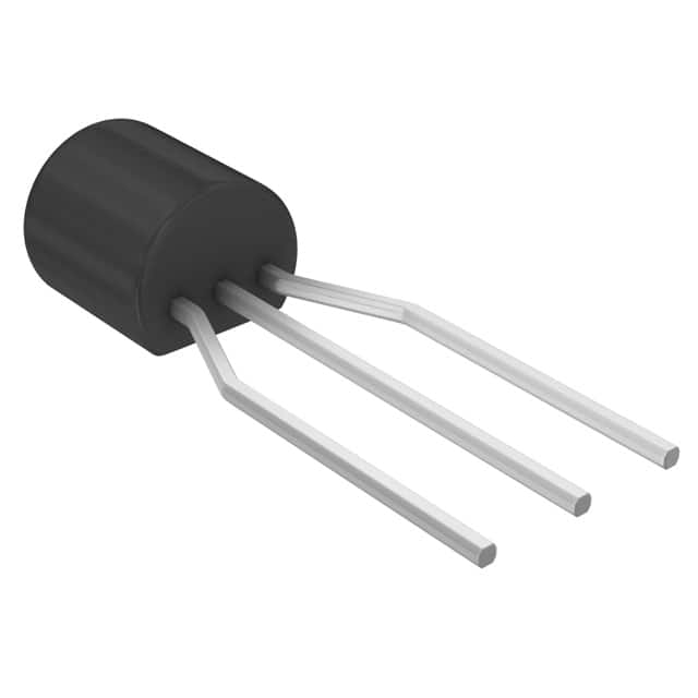
BC517ZL1
Product Overview
Category: Optoelectronics
Use: Phototransistor
Characteristics: High sensitivity, small package size
Package: SMD
Essence: Light detection and amplification
Packaging/Quantity: Tape and reel, 3000 pieces per reel
Specifications
- Collector-Emitter Voltage: 30V
- Emitter-Collector Voltage: 5V
- Collector Current: 50mA
- Power Dissipation: 150mW
- Rise Time: 15µs
- Fall Time: 7µs
Detailed Pin Configuration
The BC517ZL1 phototransistor has a three-pin configuration: 1. Collector (C) 2. Base (B) 3. Emitter (E)
Functional Features
- High sensitivity to light
- Fast response time
- Small package size for space-constrained applications
Advantages
- Suitable for low-light conditions
- Compact SMD package
- Fast switching speed
Disadvantages
- Limited collector-emitter voltage
- Limited collector current
Working Principles
The BC517ZL1 operates based on the principle of light-induced conductivity in semiconductors. When light strikes the base-emitter junction, it generates electron-hole pairs, leading to an increase in the collector current.
Detailed Application Field Plans
The BC517ZL1 is ideal for various applications, including: - Ambient light sensing in consumer electronics - Optical encoders in industrial automation - Medical devices for pulse oximetry - Proximity sensors in automotive applications
Detailed and Complete Alternative Models
- BC516: Similar characteristics with a different package type
- BPW77NA: Higher collector-emitter voltage and current rating
- PT333-3B: Enhanced sensitivity and faster response time
In conclusion, the BC517ZL1 phototransistor offers high sensitivity and fast response in a compact SMD package, making it suitable for diverse optoelectronic applications.
Word count: 274
Lista 10 Vanliga frågor och svar relaterade till tillämpningen av BC517ZL1 i tekniska lösningar
Sure, here are 10 common questions and answers related to the application of BC517ZL1 in technical solutions:
What is BC517ZL1?
- BC517ZL1 is a general-purpose PNP bipolar junction transistor (BJT) commonly used for amplification and switching applications.
What are the typical applications of BC517ZL1?
- BC517ZL1 is commonly used in audio amplifiers, signal processing circuits, and low-power switching applications.
What are the key electrical characteristics of BC517ZL1?
- The key electrical characteristics include a maximum collector current (Ic) of 100mA, a maximum collector-emitter voltage (Vce) of 45V, and a DC current gain (hfe) of 110-800.
How do I determine the appropriate biasing for BC517ZL1 in an amplifier circuit?
- The appropriate biasing for BC517ZL1 can be determined by considering the desired operating point, load requirements, and the specific amplifier configuration being used.
Can BC517ZL1 be used in high-frequency applications?
- BC517ZL1 is not typically recommended for high-frequency applications due to its limited transition frequency (ft) of around 100MHz.
What are the thermal considerations for BC517ZL1 in power dissipation applications?
- When used in power dissipation applications, it's important to consider the maximum junction temperature and the thermal resistance of the package to ensure proper heat dissipation.
Are there any specific layout considerations when using BC517ZL1 in a PCB design?
- It's important to minimize lead lengths, provide adequate thermal vias or heatsinking, and ensure proper grounding to minimize parasitic effects and maximize performance.
Can BC517ZL1 be used in low-voltage applications?
- Yes, BC517ZL1 can be used in low-voltage applications, but it's important to ensure that the operating conditions are within the specified limits to avoid saturation or other issues.
What are the typical failure modes of BC517ZL1?
- Common failure modes include thermal runaway, breakdown due to excessive voltage or current, and degradation of the semiconductor material over time.
How does BC517ZL1 compare to similar transistors in terms of performance and specifications?
- BC517ZL1 offers comparable performance to other general-purpose PNP transistors with similar specifications, but it's important to review the datasheets for specific comparisons based on the application requirements.