

Encyclopedia Entry: 74LVT16244MEA
Product Overview
Category
The 74LVT16244MEA belongs to the category of integrated circuits (ICs) and specifically falls under the family of buffer/line drivers.
Use
This product is primarily used for signal buffering and line driving applications in electronic circuits. It helps in amplifying and transmitting digital signals between different components or subsystems within a larger system.
Characteristics
- High-speed operation: The 74LVT16244MEA is designed to operate at high speeds, making it suitable for applications requiring fast data transmission.
- Low power consumption: This IC is optimized for low power consumption, making it energy-efficient and suitable for battery-powered devices.
- Wide voltage range: It can operate within a wide voltage range, allowing compatibility with various systems and devices.
- Output impedance matching: The IC provides output impedance matching, ensuring efficient signal transfer without distortion.
Package and Quantity
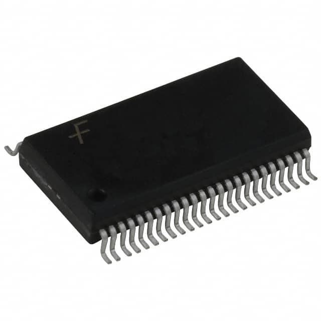
The 74LVT16244MEA is available in a standard 48-pin TSSOP (Thin Shrink Small Outline Package) package. Each package contains one IC.
Specifications
- Supply Voltage Range: 2.7V to 3.6V
- Logic Family: LVT (Low Voltage TTL)
- Number of Buffers/Drivers: 16
- Input/Output Compatibility: 3.3V CMOS/TTL
- Maximum Operating Frequency: 200 MHz
- Output Current: ±32 mA
- Propagation Delay: 4 ns (max)
Detailed Pin Configuration
The 74LVT16244MEA has a total of 48 pins, which are assigned specific functions. Here is a detailed pin configuration:
- OE (Output Enable) 1
- Y1 (Output) 1
- A1 (Input) 1
- GND (Ground)
- A2 (Input) 2
- Y2 (Output) 2
- OE (Output Enable) 2
- VCC (Supply Voltage)
- Y3 (Output) 3
- A3 (Input) 3
- GND (Ground)
- A4 (Input) 4
- Y4 (Output) 4
- OE (Output Enable) 4
- VCC (Supply Voltage)
- Y5 (Output) 5
- A5 (Input) 5
- GND (Ground)
- A6 (Input) 6
- Y6 (Output) 6
- OE (Output Enable) 6
- VCC (Supply Voltage)
- Y7 (Output) 7
- A7 (Input) 7
- GND (Ground)
- A8 (Input) 8
- Y8 (Output) 8
- OE (Output Enable) 8
- VCC (Supply Voltage)
- Y9 (Output) 9
- A9 (Input) 9
- GND (Ground)
- A10 (Input) 10
- Y10 (Output) 10
- OE (Output Enable) 10
- VCC (Supply Voltage)
- Y11 (Output) 11
- A11 (Input) 11
- GND (Ground)
- A12 (Input) 12
- Y12 (Output) 12
- OE (Output Enable) 12
- VCC (Supply Voltage)
- Y13 (Output) 13
- A13 (Input) 13
- GND (Ground)
- A14 (Input) 14
- Y14 (Output) 14
Functional Features
- Bidirectional data flow: The 74LVT16244MEA supports bidirectional data transmission, allowing signals to be sent and received.
- Output enable control: The output enable (OE) pins can be used to enable or disable the outputs, providing flexibility in controlling signal flow.
- High-speed operation: With a maximum operating frequency of 200 MHz, this IC ensures efficient data transfer in high-speed applications.
Advantages and Disadvantages
Advantages
- High-speed operation enables fast data transmission.
- Low power consumption makes it suitable for energy-efficient devices.
- Wide voltage range compatibility allows integration into various systems.
- Output impedance matching ensures signal integrity.
Disadvantages
- Limited number of buffers/drivers (16) may not be sufficient for complex circuit designs.
- Propagation delay of 4 ns (max) may introduce slight delays in time-critical applications.
Working Principles
The 74LVT16244MEA operates based on the principles of digital logic.
Lista 10 Vanliga frågor och svar relaterade till tillämpningen av 74LVT16244MEA i tekniska lösningar
Sure! Here are 10 common questions and answers related to the application of 74LVT16244MEA in technical solutions:
Q: What is the 74LVT16244MEA? A: The 74LVT16244MEA is a 16-bit buffer/driver with 3-state outputs, commonly used in digital logic circuits.
Q: What is the maximum operating voltage for the 74LVT16244MEA? A: The maximum operating voltage for the 74LVT16244MEA is typically 3.6V.
Q: Can the 74LVT16244MEA be used as a level shifter? A: Yes, the 74LVT16244MEA can be used as a level shifter to convert signals between different voltage levels.
Q: What is the output current capability of the 74LVT16244MEA? A: The 74LVT16244MEA has a typical output current capability of ±32mA.
Q: Is the 74LVT16244MEA compatible with TTL logic levels? A: Yes, the 74LVT16244MEA is compatible with both TTL and CMOS logic levels.
Q: Can the 74LVT16244MEA be used in bidirectional data bus applications? A: Yes, the 74LVT16244MEA can be used in bidirectional data bus applications by enabling the direction control pin.
Q: What is the propagation delay of the 74LVT16244MEA? A: The propagation delay of the 74LVT16244MEA is typically around 3.5ns.
Q: Does the 74LVT16244MEA have built-in ESD protection? A: Yes, the 74LVT16244MEA has built-in ESD protection to safeguard against electrostatic discharge.
Q: Can the 74LVT16244MEA be used in high-speed applications? A: Yes, the 74LVT16244MEA is designed for high-speed operation and can be used in such applications.
Q: What is the package type of the 74LVT16244MEA? A: The 74LVT16244MEA is available in various package types, such as SOIC, TSSOP, and SSOP.
Please note that the answers provided here are general and may vary depending on the specific datasheet and manufacturer's specifications for the 74LVT16244MEA.