

74LCX07BQX
Product Overview
- Category: Integrated Circuit (IC)
- Use: Logic Gate Buffer/Driver
- Characteristics: Low Voltage, High-Speed, Non-Inverting
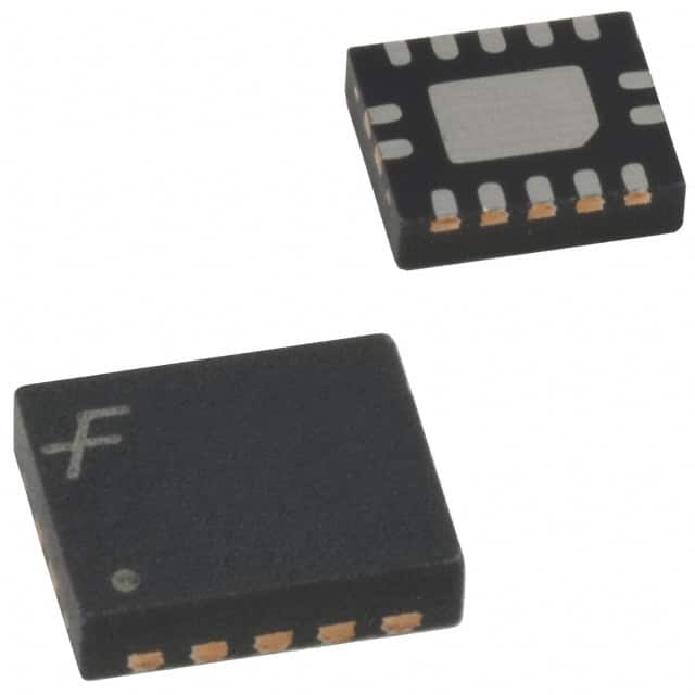
- Package: 14-pin TSSOP (Thin Shrink Small Outline Package)
- Essence: Hex Buffer/Driver with Open Drain Outputs
- Packaging/Quantity: Tape and Reel, 2500 units per reel
Specifications
- Supply Voltage Range: 1.65V to 3.6V
- Input Voltage Range: -0.5V to VCC + 0.5V
- Output Voltage Range: 0V to VCC
- Maximum Input Current: ±10mA
- Maximum Output Current: ±24mA
- Propagation Delay Time: 2.8ns (typical)
- Operating Temperature Range: -40°C to +85°C
Detailed Pin Configuration
The 74LCX07BQX has a total of 14 pins, numbered as follows:
- A1 (Input)
- Y1 (Output)
- A2 (Input)
- Y2 (Output)
- A3 (Input)
- Y3 (Output)
- GND (Ground)
- Y4 (Output)
- A4 (Input)
- Y5 (Output)
- A5 (Input)
- Y6 (Output)
- VCC (Power Supply)
- NC (No Connection)
Functional Features
- Hex Buffer/Driver: The 74LCX07BQX is equipped with six buffer/driver circuits.
- Open Drain Outputs: The outputs are designed as open drain, allowing for flexible connection configurations.
- Non-Inverting: The input signal is not inverted at the output.
Advantages and Disadvantages
Advantages: - Low Voltage Operation: The 74LCX07BQX operates at a low voltage range, making it suitable for battery-powered devices. - High-Speed Performance: With a propagation delay time of 2.8ns, this IC offers fast signal processing. - Open Drain Outputs: The open drain outputs provide versatility in connecting to other devices.
Disadvantages: - Limited Output Current: The maximum output current of ±24mA may not be sufficient for certain high-current applications. - Narrow Temperature Range: The operating temperature range of -40°C to +85°C may limit its use in extreme environments.
Working Principles
The 74LCX07BQX is a logic gate buffer/driver that amplifies and buffers digital signals. It accepts input signals from the A1 to A5 pins and provides corresponding non-inverted outputs on the Y1 to Y6 pins. The open drain outputs allow for flexible connection configurations, such as wired-OR or wired-AND setups. The IC operates within a specified voltage range and provides high-speed signal processing with minimal propagation delay.
Detailed Application Field Plans
The 74LCX07BQX finds applications in various fields, including:
- Communication Systems: Used for level shifting and signal buffering in data communication interfaces.
- Industrial Automation: Employed in control systems for signal amplification and isolation.
- Automotive Electronics: Utilized in automotive modules for voltage level conversion and signal conditioning.
- Consumer Electronics: Integrated into devices like smartphones, tablets, and gaming consoles for signal buffering and driving.
Detailed and Complete Alternative Models
- SN74LVC07A: Similar hex buffer/driver IC with non-inverting open drain outputs. Operates at a wider voltage range of 1.65V to 5.5V.
- MC74LCX07: Hex buffer/driver IC with non-inverting outputs. Operates at a voltage range of 2V to 3.6V and offers higher output current capability.
(Note: The above alternative models are provided for reference and may have different pin configurations and specifications.)
Word count: 408 words
Lista 10 Vanliga frågor och svar relaterade till tillämpningen av 74LCX07BQX i tekniska lösningar
Sure! Here are 10 common questions and answers related to the application of 74LCX07BQX in technical solutions:
Question: What is the 74LCX07BQX?
Answer: The 74LCX07BQX is a hex buffer with open-drain outputs, commonly used in digital logic circuits.Question: What is the maximum operating voltage for the 74LCX07BQX?
Answer: The maximum operating voltage for the 74LCX07BQX is 3.6V.Question: Can the 74LCX07BQX be used as a level shifter?
Answer: Yes, the 74LCX07BQX can be used as a level shifter to convert signals between different voltage levels.Question: What is the typical output current capability of the 74LCX07BQX?
Answer: The typical output current capability of the 74LCX07BQX is 24mA.Question: Is the 74LCX07BQX compatible with both CMOS and TTL logic levels?
Answer: Yes, the 74LCX07BQX is compatible with both CMOS and TTL logic levels.Question: Can the 74LCX07BQX be used in high-speed applications?
Answer: Yes, the 74LCX07BQX is designed for high-speed operation and can be used in such applications.Question: Does the 74LCX07BQX have built-in protection against overvoltage?
Answer: Yes, the 74LCX07BQX has built-in protection against overvoltage conditions.Question: Can the 74LCX07BQX be used in bidirectional communication?
Answer: No, the 74LCX07BQX is a unidirectional buffer and cannot be used for bidirectional communication.Question: What is the typical propagation delay of the 74LCX07BQX?
Answer: The typical propagation delay of the 74LCX07BQX is around 3.5ns.Question: Can the 74LCX07BQX be used in automotive applications?
Answer: Yes, the 74LCX07BQX is suitable for automotive applications as it meets the required specifications for such environments.
Please note that these answers are general and may vary depending on specific datasheet information or application requirements.