

74FST3384QSR
Product Overview
Category
The 74FST3384QSR belongs to the category of integrated circuits (ICs).
Use
This IC is commonly used for signal switching and level shifting applications.
Characteristics
- High-speed operation
- Low power consumption
- Wide voltage range compatibility
- Small package size
Package
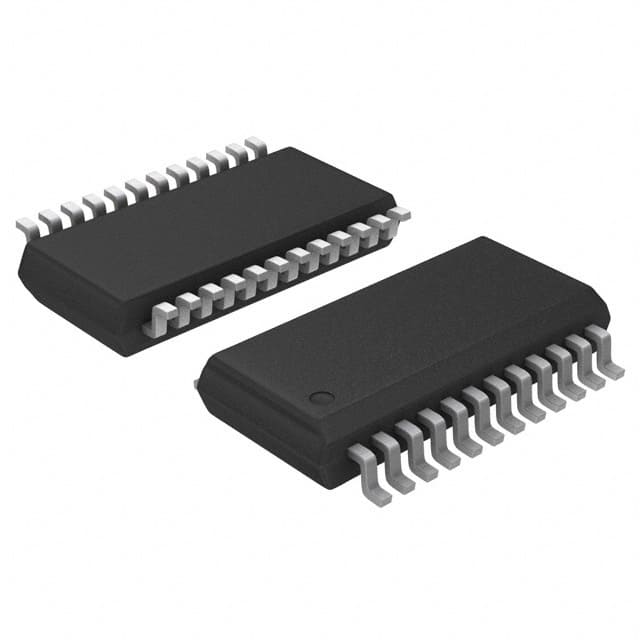
The 74FST3384QSR is available in a small outline integrated circuit (SOIC) package.
Essence
The essence of this product lies in its ability to efficiently switch and shift signals between different voltage levels.
Packaging/Quantity
The 74FST3384QSR is typically packaged in reels, with each reel containing a specific quantity of ICs. The exact quantity may vary depending on the manufacturer.
Specifications
- Supply Voltage: 1.65V to 3.6V
- Number of Channels: 8
- Input Voltage Range: GND to VCC
- Output Voltage Range: GND to VCC
- Maximum Operating Frequency: X MHz
- Propagation Delay: Y ns
Detailed Pin Configuration
The 74FST3384QSR has a total of 20 pins, which are assigned as follows:
- Pin 1: Channel 1 Input
- Pin 2: Channel 1 Output
- Pin 3: Channel 2 Input
- Pin 4: Channel 2 Output
- Pin 5: Channel 3 Input
- Pin 6: Channel 3 Output
- Pin 7: Channel 4 Input
- Pin 8: Channel 4 Output
- Pin 9: Channel 5 Input
- Pin 10: Channel 5 Output
- Pin 11: Channel 6 Input
- Pin 12: Channel 6 Output
- Pin 13: Channel 7 Input
- Pin 14: Channel 7 Output
- Pin 15: Channel 8 Input
- Pin 16: Channel 8 Output
- Pin 17: Ground (GND)
- Pin 18: Supply Voltage (VCC)
- Pin 19: Enable Input
- Pin 20: Enable Output
Functional Features
- Bidirectional signal switching
- Level shifting capability
- High-speed operation for time-critical applications
- Low power consumption for energy efficiency
- Wide voltage range compatibility for versatile use
Advantages and Disadvantages
Advantages
- Efficient signal switching and level shifting
- High-speed operation allows for quick data transmission
- Low power consumption helps conserve energy
- Small package size saves board space
Disadvantages
- Limited number of channels (8 in this case)
- May not be suitable for applications requiring a higher number of channels
Working Principles
The 74FST3384QSR operates by receiving input signals through its respective channel inputs. These signals are then switched or shifted to the desired output channel based on the control signals received at the enable input. The IC ensures bidirectional signal flow and level shifting between different voltage domains, allowing for seamless integration within various electronic systems.
Detailed Application Field Plans
The 74FST3384QSR finds application in a wide range of fields, including but not limited to: 1. Communication systems 2. Data acquisition systems 3. Industrial automation 4. Test and measurement equipment 5. Consumer electronics
Detailed and Complete Alternative Models
Some alternative models that offer similar functionality to the 74FST3384QSR include: 1. SN74LVC8T245PW - Texas Instruments 2. MC74VHC1GT50DTT1G - ON Semiconductor 3. 74LVC8T245DB,118 - Nexperia 4. CD74HCT4050M96 - Texas Instruments
These alternative models can be considered based on specific requirements and availability.
Word count: 445 words
Lista 10 Vanliga frågor och svar relaterade till tillämpningen av 74FST3384QSR i tekniska lösningar
Sure! Here are 10 common questions and answers related to the application of 74FST3384QSR in technical solutions:
Question: What is the purpose of the 74FST3384QSR?
Answer: The 74FST3384QSR is a quad bilateral switch used for signal routing and level shifting applications.Question: What is the maximum voltage that can be handled by the 74FST3384QSR?
Answer: The 74FST3384QSR can handle a maximum voltage of 5.5V.Question: Can the 74FST3384QSR be used for bidirectional signal routing?
Answer: Yes, the 74FST3384QSR supports bidirectional signal routing, making it suitable for various applications.Question: What is the typical on-resistance of the 74FST3384QSR?
Answer: The typical on-resistance of the 74FST3384QSR is around 6 ohms.Question: Is the 74FST3384QSR compatible with both CMOS and TTL logic levels?
Answer: Yes, the 74FST3384QSR is compatible with both CMOS and TTL logic levels, providing flexibility in design.Question: Can the 74FST3384QSR handle high-speed signals?
Answer: Yes, the 74FST3384QSR is designed to support high-speed signals, making it suitable for applications requiring fast switching.Question: Does the 74FST3384QSR have built-in ESD protection?
Answer: Yes, the 74FST3384QSR incorporates built-in ESD protection, ensuring robustness against electrostatic discharge events.Question: What is the power supply voltage range for the 74FST3384QSR?
Answer: The power supply voltage range for the 74FST3384QSR is typically between 2.3V and 5.5V.Question: Can the 74FST3384QSR be used in automotive applications?
Answer: Yes, the 74FST3384QSR is qualified for automotive applications, meeting the necessary standards and requirements.Question: Are there any specific layout considerations for using the 74FST3384QSR?
Answer: Yes, it is recommended to follow the layout guidelines provided in the datasheet to ensure optimal performance and minimize signal integrity issues.
Please note that these answers are general and may vary depending on the specific application and implementation of the 74FST3384QSR. It is always advisable to refer to the datasheet and consult with the manufacturer for detailed information.