

Encyclopedia Entry: 74ACT533MTC
Product Overview
- Category: Integrated Circuit (IC)
- Use: Digital Logic Device
- Characteristics: High-speed, Octal Transparent Latch with 3-State Outputs
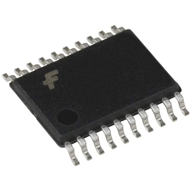
- Package: TSSOP-20
- Essence: The 74ACT533MTC is an octal transparent latch with 3-state outputs. It is designed to store and control the flow of digital data in various applications.
- Packaging/Quantity: The 74ACT533MTC is typically sold in reels or tubes containing multiple units.
Specifications
- Logic Family: ACT
- Number of Bits: 8 (Octal)
- Output Type: 3-State
- Latch Type: Transparent
- Operating Voltage Range: 4.5V to 5.5V
- Input Voltage Range: 0V to VCC
- Propagation Delay Time: 6ns (max)
- Operating Temperature Range: -40°C to +85°C
Detailed Pin Configuration
The 74ACT533MTC has a total of 20 pins arranged as follows:
+---+--+---+
   D0 --|1  +--+ 20|-- VCC
   D1 --|2         |-- GND
   D2 --|3         |-- Q0
   D3 --|4         |-- Q1
   D4 --|5         |-- Q2
   D5 --|6         |-- Q3
   D6 --|7         |-- Q4
   D7 --|8         |-- Q5
  GND --|9         |-- Q6
   OE --|10        |-- Q7
  CLK --|11        |-- LE
  GND --|12        |-- A0
   A1 --|13        |-- A2
   A3 --|14        |-- A4
   A5 --|15        |-- A6
   A7 --|16        |-- A8
  GND --|17        |-- Qn
   OE --|18        |-- Qn
  CLK --|19        |-- LE
        +----------+
Functional Features
- The 74ACT533MTC is equipped with eight transparent latches, each capable of storing a single bit of digital data.
- It features 3-state outputs, allowing the latched data to be either driven onto the output pins or placed in a high-impedance state.
- The latch is controlled by a clock signal (CLK) and a latch enable signal (LE), providing control over the storage and release of data.
- The output enable signal (OE) allows the outputs to be enabled or disabled as needed.
Advantages and Disadvantages
Advantages: - High-speed operation makes it suitable for applications requiring fast data transfer. - Octal configuration provides flexibility in handling multiple bits of data simultaneously. - 3-state outputs allow for efficient bus sharing and interfacing with other devices.
Disadvantages: - Limited voltage range may restrict its use in certain applications. - Propagation delay time may introduce timing constraints in critical systems.
Working Principles
The 74ACT533MTC operates based on the principles of digital logic. When the latch enable (LE) signal is active and the clock (CLK) signal transitions from low to high, the data present at the inputs (D0-D7) is latched and stored in the corresponding flip-flops. The stored data can then be accessed through the 3-state outputs (Q0-Q7) when the output enable (OE) signal is active.
Detailed Application Field Plans
The 74ACT533MTC can be used in various applications, including: 1. Data storage and retrieval systems 2. Address decoding circuits 3. Bus interface units 4. Memory modules 5. Digital communication systems
Detailed and Complete Alternative Models
Some alternative models that offer similar functionality to the 74ACT533MTC include: - 74HC533: High-speed CMOS octal transparent latch - 74LS533: Low-power Schottky TTL octal transparent latch - CD74ACT533: Advanced CMOS octal transparent latch
These alternatives may differ in terms of voltage range, speed, power consumption, and other specifications. It is important to select the appropriate model based on specific application requirements.
Word Count: 436 words
Lista 10 Vanliga frågor och svar relaterade till tillämpningen av 74ACT533MTC i tekniska lösningar
Sure! Here are 10 common questions and answers related to the application of 74ACT533MTC in technical solutions:
Q: What is the 74ACT533MTC? A: The 74ACT533MTC is a octal transparent latch with 3-state outputs, commonly used in digital circuits.
Q: What is the purpose of the 74ACT533MTC? A: The purpose of this IC is to store and control the flow of data in a digital system.
Q: How many latch outputs does the 74ACT533MTC have? A: The 74ACT533MTC has eight latch outputs, labeled from Q0 to Q7.
Q: Can the 74ACT533MTC be used as a bidirectional buffer? A: No, the 74ACT533MTC is not designed for bidirectional buffering. It only supports unidirectional data flow.
Q: What is the maximum operating voltage for the 74ACT533MTC? A: The maximum operating voltage for this IC is typically 5.5V.
Q: How does the 74ACT533MTC handle input data? A: The 74ACT533MTC has a transparent latch design, which means that the input data is directly transferred to the output when the latch enable (LE) signal is high.
Q: Can the 74ACT533MTC drive external loads directly? A: Yes, the 74ACT533MTC has 3-state outputs that can drive external loads directly.
Q: What is the function of the output enable (OE) pin on the 74ACT533MTC? A: The OE pin is used to enable or disable the outputs of the IC. When OE is high, the outputs are enabled; when OE is low, the outputs are disabled.
Q: Can the 74ACT533MTC be cascaded to increase the number of latch outputs? A: Yes, multiple 74ACT533MTC ICs can be cascaded together to increase the number of latch outputs in a system.
Q: What is the typical propagation delay of the 74ACT533MTC? A: The typical propagation delay of this IC is around 5 ns, making it suitable for high-speed digital applications.
Please note that these answers are general and may vary depending on the specific datasheet and manufacturer's specifications for the 74ACT533MTC.