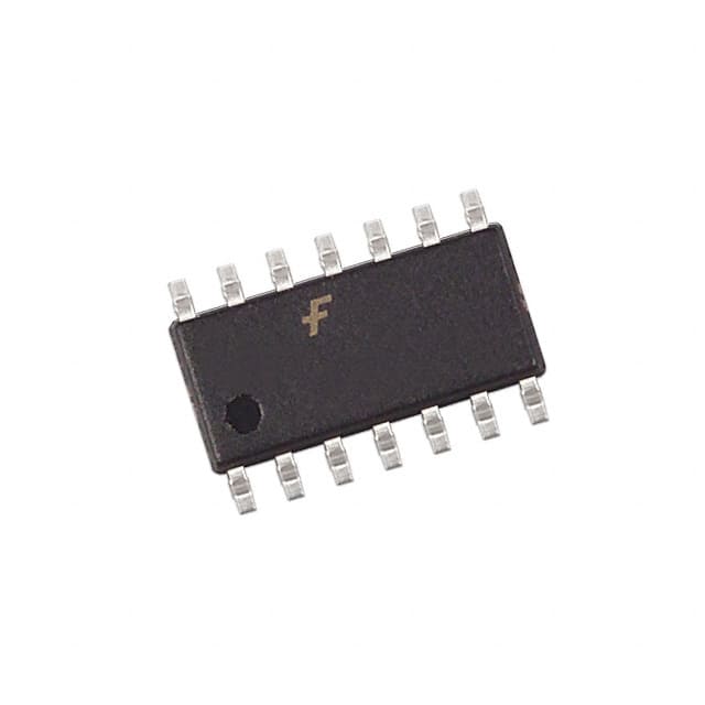
Encyclopedia Entry: 74ACT00SJX
Product Overview
Category
The 74ACT00SJX belongs to the category of integrated circuits (ICs).
Use
This IC is commonly used in digital logic applications for signal processing and data manipulation.
Characteristics
- High-speed operation
- Low power consumption
- Wide operating voltage range
- Compatibility with TTL (Transistor-Transistor Logic) inputs
- Schmitt trigger input for noise immunity
Package
The 74ACT00SJX is available in a small outline integrated circuit (SOIC) package.
Essence
The essence of the 74ACT00SJX lies in its ability to perform logical operations, specifically NAND gates, in electronic circuits.
Packaging/Quantity
The 74ACT00SJX is typically packaged in reels or tubes, containing a quantity of 250 or 300 units per package.
Specifications
- Supply Voltage Range: 4.5V to 5.5V
- Input Voltage Range: 0V to VCC
- Output Voltage Range: 0V to VCC
- Operating Temperature Range: -40°C to +85°C
- Propagation Delay Time: 3.8ns (typical)
- Maximum Quiescent Current: 4mA
Detailed Pin Configuration
The 74ACT00SJX has a total of 14 pins, numbered as follows:
- Pin 1: A Input
- Pin 2: B Input
- Pin 3: Y Output
- Pin 4: GND (Ground)
- Pin 5: C Input
- Pin 6: D Input
- Pin 7: Y Output
- Pin 8: VCC (Supply Voltage)
- Pin 9: E Input
- Pin 10: F Input
- Pin 11: Y Output
- Pin 12: H Input
- Pin 13: I Input
- Pin 14: Y Output
Functional Features
The 74ACT00SJX is a quad 2-input NAND gate IC. It performs the logical operation of a NAND gate on each of its four independent gates. The inputs and outputs are compatible with TTL logic levels, making it suitable for interfacing with other digital circuits.
Advantages and Disadvantages
Advantages
- High-speed operation allows for efficient data processing.
- Low power consumption helps conserve energy in electronic systems.
- Wide operating voltage range provides flexibility in various applications.
- Compatibility with TTL inputs enables seamless integration with existing circuitry.
- Schmitt trigger input ensures reliable operation in noisy environments.
Disadvantages
- Limited number of gates per IC may require multiple devices for complex logic functions.
- Propagation delay time may introduce timing issues in certain applications.
Working Principles
The 74ACT00SJX operates based on the principles of semiconductor technology. It utilizes transistors and other electronic components to implement the logical NAND function. When appropriate input signals are applied, the internal circuitry of the IC performs the necessary operations to produce the desired output.
Detailed Application Field Plans
The 74ACT00SJX finds application in various fields, including but not limited to: - Digital signal processing - Microcontroller-based systems - Data communication - Industrial automation - Consumer electronics
Detailed and Complete Alternative Models
Some alternative models that offer similar functionality to the 74ACT00SJX include: - 74HC00: A CMOS version of the NAND gate IC with higher supply voltage tolerance. - 74LS00: A low-power Schottky version of the NAND gate IC with lower power consumption. - CD4011: A complementary metal-oxide-semiconductor (CMOS) NAND gate IC with higher noise immunity.
These alternative models can be considered based on specific requirements and compatibility with the existing circuitry.
Word count: 550 words
Lista 10 Vanliga frågor och svar relaterade till tillämpningen av 74ACT00SJX i tekniska lösningar
Sure! Here are 10 common questions and answers related to the application of 74ACT00SJX in technical solutions:
Q: What is the 74ACT00SJX? A: The 74ACT00SJX is a quad 2-input NAND gate integrated circuit (IC) commonly used in digital logic circuits.
Q: What is the operating voltage range of 74ACT00SJX? A: The operating voltage range of 74ACT00SJX is typically between 4.5V and 5.5V.
Q: What is the maximum input voltage for 74ACT00SJX? A: The maximum input voltage for 74ACT00SJX is equal to the supply voltage, which is typically 5.5V.
Q: What is the output current capability of 74ACT00SJX? A: The output current capability of 74ACT00SJX is typically around 24mA.
Q: Can 74ACT00SJX be used as a level shifter? A: Yes, 74ACT00SJX can be used as a level shifter to convert signals between different voltage levels.
Q: How many gates are there in a single 74ACT00SJX IC? A: A single 74ACT00SJX IC contains four independent NAND gates.
Q: What is the propagation delay of 74ACT00SJX? A: The propagation delay of 74ACT00SJX is typically around 5 nanoseconds.
Q: Can 74ACT00SJX be used in high-speed applications? A: Yes, 74ACT00SJX is designed for high-speed operation and can be used in applications requiring fast switching.
Q: Is 74ACT00SJX compatible with other logic families? A: Yes, 74ACT00SJX is compatible with a wide range of logic families, including TTL and CMOS.
Q: What are some common applications of 74ACT00SJX? A: Some common applications of 74ACT00SJX include digital signal processing, data communication systems, and general-purpose digital logic circuits.
Please note that the answers provided here are general and may vary depending on specific datasheet specifications and application requirements.


