

P89V51RD2FN,112
Basic Information Overview
- Category: Microcontroller
- Use: Embedded systems, industrial automation, consumer electronics
- Characteristics: 8-bit microcontroller, high-performance, low-power consumption
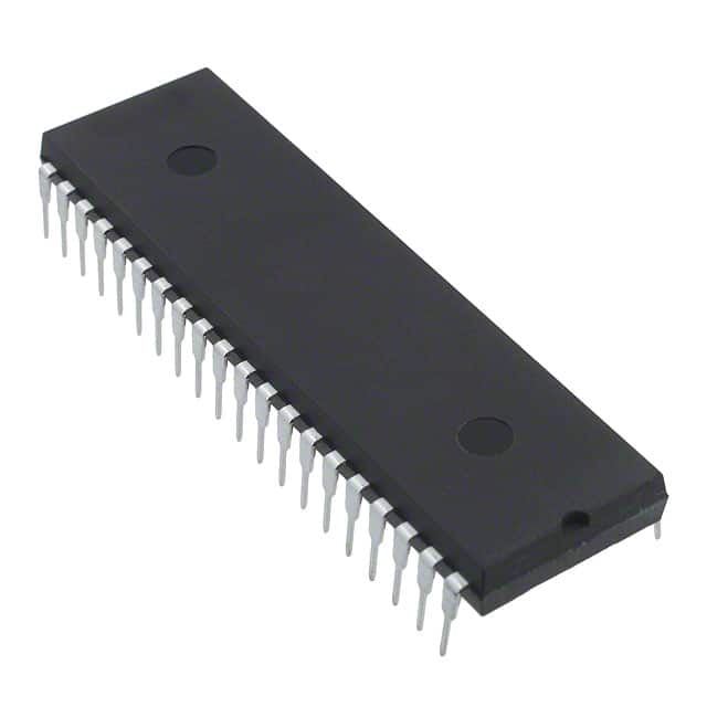
- Package: Plastic Dual In-line Package (PDIP)
- Essence: Central processing unit for controlling electronic devices
- Packaging/Quantity: Bulk packaging, quantity varies
Specifications
- Architecture: 8051
- CPU Speed: Up to 40 MHz
- Program Memory Size: 64 KB
- RAM Size: 1 KB
- Data EEPROM Size: 512 bytes
- I/O Pins: 32
- Timers/Counters: 3
- Serial Communication: UART, SPI, I2C
- ADC Channels: 8
- Operating Voltage: 2.7 V to 5.5 V
Detailed Pin Configuration
The P89V51RD2FN,112 microcontroller has a total of 40 pins. Here is the detailed pin configuration:
- P0.0 - Port 0, Pin 0
- P0.1 - Port 0, Pin 1
- P0.2 - Port 0, Pin 2
- P0.3 - Port 0, Pin 3
- P0.4 - Port 0, Pin 4
- P0.5 - Port 0, Pin 5
- P0.6 - Port 0, Pin 6
- P0.7 - Port 0, Pin 7
- RST - Reset Pin
- P1.0 - Port 1, Pin 0
- P1.1 - Port 1, Pin 1
- P1.2 - Port 1, Pin 2
- P1.3 - Port 1, Pin 3
- P1.4 - Port 1, Pin 4
- P1.5 - Port 1, Pin 5
- P1.6 - Port 1, Pin 6
- P1.7 - Port 1, Pin 7
- XTAL1 - Crystal Oscillator Input
- XTAL2 - Crystal Oscillator Output
- GND - Ground
- VCC - Power Supply
- P2.0 - Port 2, Pin 0
- P2.1 - Port 2, Pin 1
- P2.2 - Port 2, Pin 2
- P2.3 - Port 2, Pin 3
- P2.4 - Port 2, Pin 4
- P2.5 - Port 2, Pin 5
- P2.6 - Port 2, Pin 6
- P2.7 - Port 2, Pin 7
- ALE/PROG - Address Latch Enable/Program Pin
- PSEN - Program Store Enable Pin
- EA/VPP - External Access Enable/Voltage Programming Pin
- P3.0 - Port 3, Pin 0
- P3.1 - Port 3, Pin 1
- P3.2 - Port 3, Pin 2
- P3.3 - Port 3, Pin 3
- P3.4 - Port 3, Pin 4
- P3.5 - Port 3, Pin 5
- P3.6 - Port 3, Pin 6
- P3.7 - Port 3, Pin 7
Functional Features
- High-performance 8-bit microcontroller with an 8051 architecture.
- Supports a wide range of communication protocols such as UART, SPI, and I2C.
- Integrated analog-to-digital converter (ADC) for sensor interfacing.
- Flexible I/O pins for connecting external devices.
- Low-power consumption for energy-efficient applications.
- On-chip program memory and data EEPROM for storing code and data.
Advantages and Disadvantages
Advantages: - Powerful and versatile microcontroller suitable for various applications. - Extensive support and documentation available due to the popularity of the 8051 architecture. - Low-power consumption makes it ideal for battery-powered devices. - Integrated ADC simplifies analog signal processing.
Disadvantages: - Limited program memory size compared to modern microcontrollers. - Limited RAM size may restrict complex data manipulation. - Lack of advanced features found in more recent microcontroller architectures.
Working Principles
The P89V51RD2FN,112 microcontroller operates based on the 8051 architecture. It executes instructions stored in its program memory and
Lista 10 Vanliga frågor och svar relaterade till tillämpningen av P89V51RD2FN,112 i tekniska lösningar
Sure! Here are 10 common questions and answers related to the application of P89V51RD2FN,112 in technical solutions:
Q: What is P89V51RD2FN,112? A: P89V51RD2FN,112 is a microcontroller from NXP Semiconductors based on the 8051 architecture.
Q: What are the key features of P89V51RD2FN,112? A: Some key features include 8KB Flash memory, 128 bytes of RAM, 32 I/O pins, UART, SPI, and I2C interfaces.
Q: Can I program P89V51RD2FN,112 using C or assembly language? A: Yes, you can program P89V51RD2FN,112 using both C and assembly language.
Q: How do I program P89V51RD2FN,112? A: You can use an ISP (In-System Programming) tool or a compatible programmer to program the microcontroller.
Q: What voltage does P89V51RD2FN,112 operate at? A: P89V51RD2FN,112 operates at a voltage range of 2.7V to 5.5V.
Q: Can I use P89V51RD2FN,112 in battery-powered applications? A: Yes, P89V51RD2FN,112 can be used in battery-powered applications due to its low power consumption.
Q: Does P89V51RD2FN,112 have any built-in peripherals? A: Yes, it has built-in peripherals such as timers/counters, PWM, ADC, and external interrupt support.
Q: Can I interface P89V51RD2FN,112 with other devices or sensors? A: Yes, P89V51RD2FN,112 supports various communication interfaces like UART, SPI, and I2C, allowing easy interfacing with other devices.
Q: Is P89V51RD2FN,112 suitable for real-time applications? A: Yes, P89V51RD2FN,112 can be used in real-time applications due to its interrupt handling capabilities and timers/counters.
Q: Are there any development tools available for P89V51RD2FN,112? A: Yes, NXP provides development tools like IDEs (Integrated Development Environments) and compilers specifically designed for programming P89V51RD2FN,112.
Please note that these answers are general and may vary depending on the specific requirements and use cases of your technical solution.