

P89V51RD2FA,512
Basic Information Overview
- Category: Microcontroller
- Use: Embedded systems and applications
- Characteristics:
- 8-bit microcontroller
- Flash-based program memory
- High-performance CPU
- Wide range of peripherals
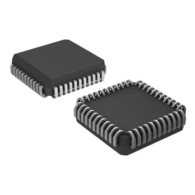
- Package: 40-pin Dual In-Line Package (DIP)
- Essence: Versatile microcontroller for various embedded applications
- Packaging/Quantity: Available in individual units or reels
Specifications
- Architecture: 8051
- CPU Speed: Up to 33 MHz
- Program Memory: 64 KB Flash
- Data Memory: 1 KB RAM
- I/O Pins: 32
- Timers/Counters: 3
- Serial Communication: UART, SPI, I2C
- Analog-to-Digital Converter (ADC): 8 channels, 10-bit resolution
- Operating Voltage: 2.7V to 5.5V
- Operating Temperature: -40°C to +85°C
Detailed Pin Configuration
The P89V51RD2FA,512 microcontroller has a total of 40 pins. The pin configuration is as follows:
- P0.0 / AD0 / RXD
- P0.1 / AD1 / TXD
- P0.2 / AD2 / INT0
- P0.3 / AD3 / INT1
- P0.4 / AD4 / T0
- P0.5 / AD5 / T1
- P0.6 / AD6 / WR
- P0.7 / AD7 / RD
- RST
- P1.0 / T2
- P1.1 / T2EX
- P1.2 / WR
- P1.3 / RD
- P1.4 / T0
- P1.5 / T1
- P1.6 / XTAL2
- P1.7 / XTAL1
- AVSS
- ALE / PROG
- EA / VPP
- P2.0 / A8
- P2.1 / A9
- P2.2 / A10
- P2.3 / A11
- P2.4 / A12
- P2.5 / A13
- P2.6 / A14
- P2.7 / A15
- PSEN
- P3.0 / RXD
- P3.1 / TXD
- P3.2 / INT0
- P3.3 / INT1
- P3.4 / T0
- P3.5 / T1
- P3.6 / WR
- P3.7 / RD
- XTAL2
- XTAL1
- VCC
Functional Features
- High-performance 8051 CPU core
- Flash-based program memory allows easy reprogramming
- Wide range of peripherals for versatile applications
- Multiple serial communication interfaces (UART, SPI, I2C)
- On-chip analog-to-digital converter (ADC) for sensor interfacing
- Timers and counters for precise timing operations
- Interrupt support for efficient event handling
- Low power consumption in idle mode
Advantages
- Versatile microcontroller suitable for various embedded applications
- Ample program memory for complex firmware development
- Extensive peripheral options for flexible system design
- Support for multiple serial communication protocols simplifies integration
- On-chip ADC enables direct sensor interfacing
- Low power consumption extends battery life in portable devices
Disadvantages
- Limited RAM size may restrict data-intensive applications
- 8-bit architecture may not be suitable for computationally intensive tasks
- Lack of advanced features found in more modern microcontrollers
- Availability and support may vary depending on the region
Working Principles
The P89V51RD2FA,512 microcontroller is based on the 8051 architecture. It operates by executing instructions stored in its Flash program memory. The CPU core performs arithmetic, logical, and control operations to process data and control external peripherals. The microcontroller communicates with other devices through its I/O pins and serial communication interfaces. Interrupts are used to handle time-critical events, ensuring efficient operation.
Detailed Application Field Plans
The P89V51RD2FA,512 microcontroller finds applications in various fields, including: - Industrial automation - Home automation - Automotive electronics - Consumer electronics - Medical devices - Internet of Things (IoT) devices
Detailed and Complete Alternative Models
Some alternative microcontrollers that can
Lista 10 Vanliga frågor och svar relaterade till tillämpningen av P89V51RD2FA,512 i tekniska lösningar
Sure! Here are 10 common questions and answers related to the application of P89V51RD2FA,512 in technical solutions:
Q: What is P89V51RD2FA,512? A: P89V51RD2FA,512 is a microcontroller from NXP Semiconductors based on the 8051 architecture.
Q: What are the key features of P89V51RD2FA,512? A: Some key features include 64KB Flash memory, 1024 bytes of RAM, 32 I/O pins, UART, SPI, and I2C interfaces.
Q: How can I program P89V51RD2FA,512? A: You can program it using an ISP (In-System Programming) tool or through a serial bootloader.
Q: Can I use C language for programming P89V51RD2FA,512? A: Yes, you can use C language along with the Keil C51 compiler or other compatible compilers.
Q: What voltage levels does P89V51RD2FA,512 support? A: It supports a wide range of voltage levels, typically from 2.7V to 5.5V.
Q: How many timers/counters are available in P89V51RD2FA,512? A: It has two 16-bit timers/counters (Timer 0 and Timer 1) with various operating modes.
Q: Can I interface P89V51RD2FA,512 with external memory? A: Yes, it supports external memory interfacing through its address and data bus.
Q: Does P89V51RD2FA,512 have any built-in communication interfaces? A: Yes, it has a UART (Universal Asynchronous Receiver/Transmitter) for serial communication.
Q: Can P89V51RD2FA,512 be used in industrial applications? A: Yes, it is suitable for various industrial applications due to its robustness and reliability.
Q: Are there any development boards available for P89V51RD2FA,512? A: Yes, there are development boards specifically designed for P89V51RD2FA,512 that provide easy prototyping and testing capabilities.
Please note that these answers are general and may vary depending on the specific requirements and implementation of the technical solution.