

N74F543DB,118
Basic Information Overview
- Category: Integrated Circuit (IC)
- Use: Logic Level Shifter
- Characteristics: High-speed, Non-inverting, Octal D-type Flip-Flop
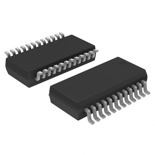
- Package: SSOP (Shrink Small Outline Package)
- Essence: Logic level shifting and flip-flop functionality in a single IC
- Packaging/Quantity: Tape and Reel, 2500 units per reel
Specifications
- Supply Voltage Range: 2.0V to 6.0V
- Input Voltage Range: GND to VCC
- Output Voltage Range: GND to VCC
- Operating Temperature Range: -40°C to +85°C
- Propagation Delay Time: 4.5ns (typical)
- Output Current: ±24mA
- Input Capacitance: 3pF (typical)
- Output Capacitance: 8pF (typical)
Detailed Pin Configuration
- OE (Output Enable)
- CP (Clock Pulse)
- D0 (Data Input 0)
- D1 (Data Input 1)
- D2 (Data Input 2)
- D3 (Data Input 3)
- D4 (Data Input 4)
- D5 (Data Input 5)
- D6 (Data Input 6)
- D7 (Data Input 7)
- Q0 (Flip-Flop Output 0)
- Q1 (Flip-Flop Output 1)
- Q2 (Flip-Flop Output 2)
- Q3 (Flip-Flop Output 3)
- Q4 (Flip-Flop Output 4)
- Q5 (Flip-Flop Output 5)
- Q6 (Flip-Flop Output 6)
- Q7 (Flip-Flop Output 7)
- GND (Ground)
- VCC (Supply Voltage)
Functional Features
- Non-inverting octal D-type flip-flop with output enable
- High-speed operation suitable for various applications
- Logic level shifting capability allows interfacing between different voltage domains
- Output enable pin provides control over the output state
Advantages and Disadvantages
Advantages
- High-speed operation enables efficient data processing
- Non-inverting functionality simplifies circuit design
- Octal configuration allows handling multiple data inputs simultaneously
- Logic level shifting capability enhances compatibility between different voltage levels
Disadvantages
- Limited supply voltage range (2.0V to 6.0V)
- Propagation delay time may affect timing-sensitive applications
- SSOP package may require careful handling during assembly
Working Principles
The N74F543DB,118 is a non-inverting octal D-type flip-flop with output enable. It operates by capturing the input data on the rising edge of the clock pulse (CP) and storing it in the flip-flop registers. The stored data is then available at the respective output pins (Q0-Q7). The output enable (OE) pin controls the state of the outputs, allowing them to be enabled or disabled as required. The logic level shifting capability ensures seamless communication between devices operating at different voltage levels.
Detailed Application Field Plans
The N74F543DB,118 finds application in various fields where logic level shifting and flip-flop functionality are required. Some potential application areas include: 1. Microcontroller interfacing with different voltage peripherals 2. Data transmission between systems operating at different voltage domains 3. Memory address decoding and data storage in digital systems 4. Signal conditioning and level conversion in communication systems 5. Industrial automation and control systems requiring reliable data storage and transfer
Detailed and Complete Alternative Models
- SN74LVCC3245A: Low-Voltage Octal Bus Transceiver with 3-State Outputs
- CD4508B: CMOS Dual 4-Bit Latch/Shift Register
- MC74HC574ADW: High-Speed CMOS Octal D-Type Flip-Flop with 3-State Outputs
- 74HCT273: Octal D-type flip-flop; positive-edge trigger; 3-state
(Note: The above list is not exhaustive and serves as a reference for alternative models.)
This entry provides an overview of the N74F543DB,118 integrated circuit, including its basic information, specifications, pin configuration, functional features, advantages and disadvantages, working principles, application field plans, and alternative models. With its logic level shifting and flip-flop capabilities, this IC offers versatility in various digital systems and communication applications.
Lista 10 Vanliga frågor och svar relaterade till tillämpningen av N74F543DB,118 i tekniska lösningar
Sure! Here are 10 common questions and answers related to the application of N74F543DB,118 in technical solutions:
Q: What is the N74F543DB,118? A: The N74F543DB,118 is a octal transceiver with tri-state outputs, designed for bus-oriented applications.
Q: What is the maximum operating voltage for the N74F543DB,118? A: The maximum operating voltage for the N74F543DB,118 is 5.5V.
Q: How many channels does the N74F543DB,118 have? A: The N74F543DB,118 has 8 channels or bits.
Q: What is the purpose of the tri-state outputs in the N74F543DB,118? A: The tri-state outputs allow the user to disable the outputs, effectively disconnecting them from the bus.
Q: Can the N74F543DB,118 be used bidirectionally? A: Yes, the N74F543DB,118 can be used for bidirectional data transfer.
Q: What is the maximum frequency at which the N74F543DB,118 can operate? A: The N74F543DB,118 can operate at a maximum frequency of 100MHz.
Q: Does the N74F543DB,118 have any built-in protection features? A: Yes, the N74F543DB,118 has built-in ESD protection on all inputs and outputs.
Q: Can the N74F543DB,118 be cascaded to increase the number of channels? A: Yes, multiple N74F543DB,118 devices can be cascaded together to increase the number of channels.
Q: What is the power supply voltage range for the N74F543DB,118? A: The power supply voltage range for the N74F543DB,118 is typically between 4.5V and 5.5V.
Q: Is the N74F543DB,118 compatible with other logic families? A: Yes, the N74F543DB,118 is compatible with a wide range of logic families, including TTL, CMOS, and LVTTL.
Please note that these answers are general and may vary depending on the specific datasheet and application requirements.