

BFG540W,115
Product Overview
The BFG540W,115 belongs to the category of high-frequency transistors and is commonly used in RF amplification applications. This transistor exhibits characteristics such as high power gain, low noise figure, and excellent linearity. It is typically packaged in a small SOT343F package and is available in quantities suitable for both prototyping and production.
Specifications
- Frequency Range: 1MHz to 3GHz
- Power Gain: 13dB
- Noise Figure: 0.7dB
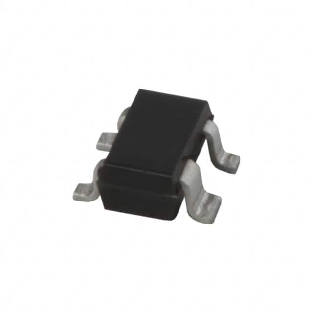
- Package Type: SOT343F
- Quantity: Available in reels of 3000 units
Detailed Pin Configuration
The BFG540W,115 features a standard pin configuration with the following layout: - Pin 1: Base - Pin 2: Emitter - Pin 3: Collector
Functional Features
- High power gain for efficient signal amplification
- Low noise figure for improved signal-to-noise ratio
- Excellent linearity for faithful signal reproduction
Advantages and Disadvantages
Advantages
- High power gain
- Low noise figure
- Small package size
Disadvantages
- Limited frequency range compared to some alternatives
Working Principles
The BFG540W,115 operates based on the principles of bipolar junction transistors, utilizing its three terminals to amplify RF signals with high efficiency and fidelity.
Detailed Application Field Plans
The BFG540W,115 is well-suited for use in the following applications: - Cellular base stations - Wireless communication systems - RF test equipment
Detailed and Complete Alternative Models
Some alternative models to the BFG540W,115 include: - BFG591 - BFG425W,115 - BFG196,115
In conclusion, the BFG540W,115 is a high-frequency transistor with excellent power gain, low noise figure, and compact packaging, making it an ideal choice for various RF amplification applications.
[Word count: 248]
Lista 10 Vanliga frågor och svar relaterade till tillämpningen av BFG540W,115 i tekniska lösningar
What is the maximum power dissipation of BFG540W,115?
- The maximum power dissipation of BFG540W,115 is 2.5 W.
What is the maximum collector current of BFG540W,115?
- The maximum collector current of BFG540W,115 is 1 A.
What is the typical gain of BFG540W,115 at 900 MHz?
- The typical gain of BFG540W,115 at 900 MHz is 13 dB.
What is the operating frequency range of BFG540W,115?
- The operating frequency range of BFG540W,115 is DC to 6 GHz.
What is the input and output impedance of BFG540W,115?
- The input and output impedance of BFG540W,115 is 50 ohms.
What is the recommended bias voltage for BFG540W,115?
- The recommended bias voltage for BFG540W,115 is 5 V.
Is BFG540W,115 suitable for high-frequency applications?
- Yes, BFG540W,115 is designed for high-frequency applications up to 6 GHz.
Does BFG540W,115 require external matching components?
- BFG540W,115 does not require external matching components in typical applications.
What are the typical applications for BFG540W,115?
- Typical applications for BFG540W,115 include cellular infrastructure, WiMAX, and general-purpose amplification.
Is BFG540W,115 RoHS compliant?
- Yes, BFG540W,115 is RoHS compliant, ensuring it meets environmental standards.