

74HCT7403D,512
Basic Information Overview
- Category: Integrated Circuit (IC)
- Use: Logic Gate
- Characteristics: High-speed, low-power consumption
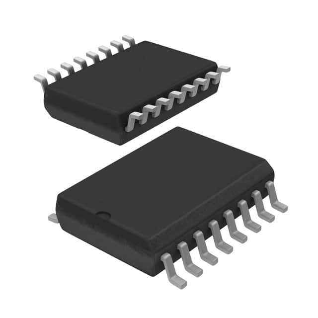
- Package: SOIC (Small Outline Integrated Circuit)
- Essence: Quad 2-input NAND gate
- Packaging/Quantity: Tape and Reel, 2500 pieces per reel
Specifications
- Supply Voltage Range: 2.0V to 6.0V
- Input Voltage Range: 0V to VCC
- Output Voltage Range: 0V to VCC
- Operating Temperature Range: -40°C to +125°C
- Propagation Delay Time: 10 ns (typical)
Detailed Pin Configuration
The 74HCT7403D,512 has a total of 14 pins. The pin configuration is as follows:
- A1 (Input A1)
- B1 (Input B1)
- Y1 (Output Y1)
- GND (Ground)
- A2 (Input A2)
- B2 (Input B2)
- Y2 (Output Y2)
- VCC (Supply Voltage)
- A3 (Input A3)
- B3 (Input B3)
- Y3 (Output Y3)
- NC (No Connection)
- A4 (Input A4)
- B4 (Input B4)
Functional Features
- Quad 2-input NAND gate with open-drain outputs
- Compatible with TTL levels
- Schmitt-trigger action on all inputs
- Balanced propagation delays
- Low power consumption
- High noise immunity
Advantages and Disadvantages
Advantages: - High-speed operation - Low power consumption - Wide supply voltage range - Schmitt-trigger action for improved noise immunity
Disadvantages: - Open-drain outputs may require additional pull-up resistors - Limited number of inputs and outputs
Working Principles
The 74HCT7403D,512 is a quad 2-input NAND gate with open-drain outputs. It operates by performing the logical NAND operation on the inputs A1/B1, A2/B2, A3/B3, and A4/B4. The output Y1/Y2/Y3 will be low (logic 0) only when both inputs are high (logic 1). The open-drain outputs allow for wired-OR connections and can be used to drive external devices.
Detailed Application Field Plans
The 74HCT7403D,512 can be used in various applications, including: - Digital logic circuits - Data processing systems - Communication systems - Industrial control systems - Automotive electronics
Detailed and Complete Alternative Models
Some alternative models that can be considered as replacements for the 74HCT7403D,512 are: - SN74HCT00N - CD4011BE - MC74HC00AN - 74LS00
These alternatives offer similar functionality and can be used interchangeably depending on the specific requirements of the application.
In conclusion, the 74HCT7403D,512 is a high-speed, low-power quad 2-input NAND gate IC. It offers balanced propagation delays, wide supply voltage range, and compatibility with TTL levels. Its open-drain outputs and Schmitt-trigger action make it suitable for various digital logic applications.
Lista 10 Vanliga frågor och svar relaterade till tillämpningen av 74HCT7403D,512 i tekniska lösningar
Sure! Here are 10 common questions and answers related to the application of 74HCT7403D,512 in technical solutions:
Q: What is the function of the 74HCT7403D,512? A: The 74HCT7403D,512 is a quad 2-input NAND gate with open-drain outputs.
Q: What is the voltage supply range for this IC? A: The voltage supply range for the 74HCT7403D,512 is typically between 4.5V and 5.5V.
Q: Can I use this IC in a 3.3V system? A: Yes, the 74HCT7403D,512 is compatible with both 5V and 3.3V systems.
Q: How many gates are there in a single 74HCT7403D,512 package? A: There are four NAND gates in a single 74HCT7403D,512 package.
Q: What is the maximum output current of each gate? A: The maximum output current per gate is typically around 4mA.
Q: Can I connect the outputs of multiple gates together? A: Yes, you can connect the outputs of multiple gates together to create more complex logic functions.
Q: What is the propagation delay of the 74HCT7403D,512? A: The propagation delay is typically around 15ns.
Q: Can I use this IC in high-speed applications? A: Yes, the 74HCT7403D,512 is suitable for high-speed applications due to its low propagation delay.
Q: Is the 74HCT7403D,512 capable of driving capacitive loads? A: Yes, the outputs of this IC can drive capacitive loads up to a certain limit.
Q: Are there any special considerations for PCB layout when using this IC? A: It is recommended to follow proper PCB layout guidelines to minimize noise and ensure signal integrity.
Please note that these answers are general and may vary depending on specific application requirements.