

74LVC2G241DC,125
Basic Information Overview
- Category: Integrated Circuit (IC)
- Use: Logic Gate Buffer/Driver
- Characteristics: Low-voltage, dual gate buffer/driver with Schmitt-trigger inputs
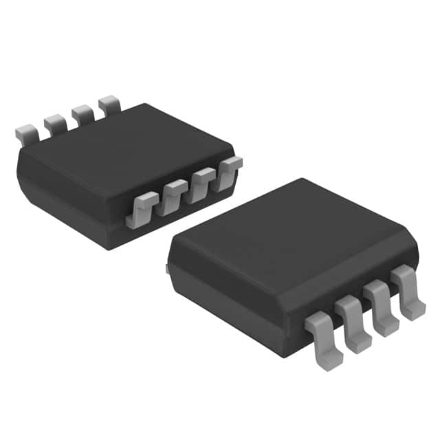
- Package: SOT753 (SC-70)
- Essence: Provides voltage level shifting and signal buffering capabilities
- Packaging/Quantity: Tape and Reel, 3000 pieces per reel
Specifications
- Supply Voltage Range: 1.65V to 5.5V
- High-Level Input Voltage: 0.7 x VCC
- Low-Level Input Voltage: 0.3 x VCC
- High-Level Output Voltage: VCC - 0.4V
- Low-Level Output Voltage: 0.4V
- Maximum Operating Frequency: 200MHz
- Propagation Delay: 4.5ns (typical)
Detailed Pin Configuration
The 74LVC2G241DC,125 IC has a total of 8 pins arranged as follows:
___________
   1 |             | 8
   2 |             | 7
   3 |             | 6
   4 |             | 5
     |_____________|
Pin Description: 1. A1: Input 1 2. Y1: Output 1 3. GND: Ground 4. A2: Input 2 5. Y2: Output 2 6. OE: Output Enable 7. VCC: Power Supply 8. NC: No Connection
Functional Features
- Dual gate buffer/driver with independent input and output pins
- Schmitt-trigger inputs for improved noise immunity
- Wide supply voltage range allows compatibility with various systems
- Low power consumption
- High-speed operation with low propagation delay
- Output enable pin for easy control of output state
Advantages and Disadvantages
Advantages: - Provides voltage level shifting capabilities - Offers signal buffering to drive capacitive loads - Schmitt-trigger inputs enhance noise immunity - Wide supply voltage range allows versatile applications - Compact package size for space-constrained designs
Disadvantages: - Limited maximum operating frequency compared to some other ICs - Not suitable for high-power applications
Working Principles
The 74LVC2G241DC,125 is a dual gate buffer/driver IC that operates as a voltage level shifter and signal buffer. It accepts two independent input signals and provides corresponding buffered outputs. The Schmitt-trigger inputs ensure reliable operation even in the presence of noise or signal fluctuations. The IC can be enabled or disabled using the OE (Output Enable) pin, allowing control over the output state.
Detailed Application Field Plans
The 74LVC2G241DC,125 finds applications in various fields, including: 1. Communication systems: Signal buffering and level shifting in data transmission circuits. 2. Industrial automation: Interface between different voltage domains in control systems. 3. Consumer electronics: Voltage translation in portable devices with multiple power supplies. 4. Automotive electronics: Signal conditioning and level shifting in automotive control modules. 5. IoT devices: Buffering and voltage conversion in sensor interfaces.
Detailed and Complete Alternative Models
Some alternative models that offer similar functionality to the 74LVC2G241DC,125 are: 1. SN74LVC2G241DBVR - Texas Instruments 2. MC74LVC2G241DTG - ON Semiconductor 3. NCV8402DTRKG - ON Semiconductor 4. TC7SZU04FUTE12L - Toshiba Semiconductor 5. 74LVC2G241GT,115 - Nexperia
These alternatives can be considered based on specific requirements and availability.
Word count: 345 words
Lista 10 Vanliga frågor och svar relaterade till tillämpningen av 74LVC2G241DC,125 i tekniska lösningar
Sure! Here are 10 common questions and answers related to the application of 74LVC2G241DC,125:
Q: What is the 74LVC2G241DC,125? A: The 74LVC2G241DC,125 is a dual buffer/line driver IC that operates at 3.3V voltage levels.
Q: What is the maximum operating frequency of the 74LVC2G241DC,125? A: The maximum operating frequency of the 74LVC2G241DC,125 is typically around 200 MHz.
Q: What is the input voltage range for the 74LVC2G241DC,125? A: The input voltage range for the 74LVC2G241DC,125 is from ground (0V) to VCC (3.3V).
Q: Can the 74LVC2G241DC,125 be used with both CMOS and TTL logic levels? A: Yes, the 74LVC2G241DC,125 is compatible with both CMOS and TTL logic levels.
Q: What is the output current capability of the 74LVC2G241DC,125? A: The 74LVC2G241DC,125 can source/sink up to 24 mA of current per channel.
Q: Does the 74LVC2G241DC,125 have internal pull-up or pull-down resistors? A: No, the 74LVC2G241DC,125 does not have internal pull-up or pull-down resistors.
Q: Can the 74LVC2G241DC,125 be used in bidirectional communication applications? A: No, the 74LVC2G241DC,125 is a unidirectional buffer/line driver and cannot be used for bidirectional communication.
Q: What is the power supply voltage range for the 74LVC2G241DC,125? A: The power supply voltage range for the 74LVC2G241DC,125 is typically from 1.65V to 3.6V.
Q: Is the 74LVC2G241DC,125 available in different package options? A: Yes, the 74LVC2G241DC,125 is available in various package options such as SOT23 and XSON.
Q: Can the 74LVC2G241DC,125 be used in automotive applications? A: Yes, the 74LVC2G241DC,125 is AEC-Q100 qualified and can be used in automotive applications.
Please note that the answers provided here are general and may vary depending on the specific datasheet and manufacturer's specifications of the 74LVC2G241DC,125.