

Encyclopedia Entry: 74LVC1G99GD,125
Product Overview
- Category: Integrated Circuit (IC)
- Use: Logic Gate
- Characteristics: Single Buffer/Driver with Open Drain Output
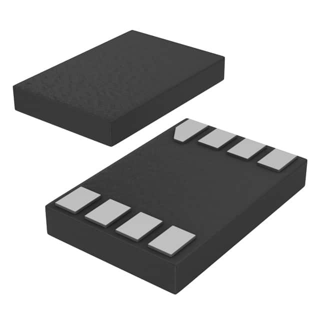
- Package: SOT753 (SC-70)
- Essence: High-Speed CMOS Technology
- Packaging/Quantity: Tape and Reel, 3000 pieces per reel
Specifications
- Supply Voltage Range: 1.65V to 5.5V
- Input Voltage Range: -0.5V to VCC + 0.5V
- Output Voltage Range: -0.5V to VCC + 0.5V
- Operating Temperature Range: -40°C to +125°C
- Propagation Delay: 3.8 ns (typical) at 2.7V
- Output Current: ±32 mA
Detailed Pin Configuration
The 74LVC1G99GD,125 IC has the following pin configuration:
____
   A1 |    | VCC
   B1 |    | Y1
 GND1 |____| OE
Functional Features
- Single buffer/driver with open drain output
- Provides a high-speed interface between different logic levels
- Supports bidirectional voltage level translation
- Allows connection of devices operating at different voltage levels
- Enables interfacing between low-voltage and higher-voltage systems
Advantages
- Wide supply voltage range allows compatibility with various systems
- High-speed CMOS technology ensures fast data transmission
- Small package size (SOT753) saves board space
- Open drain output provides flexibility in connecting to other devices
- Low power consumption enhances energy efficiency
Disadvantages
- Limited output current may restrict use in certain applications
- Not suitable for high-power or high-voltage applications
Working Principles
The 74LVC1G99GD,125 is based on high-speed CMOS technology. It operates as a single buffer/driver with an open drain output. The IC acts as a voltage level translator, allowing bidirectional communication between devices operating at different voltage levels. When the output enable (OE) pin is low, the input signal is transmitted to the output pin (Y1). When OE is high, the output pin is in a high-impedance state.
Detailed Application Field Plans
The 74LVC1G99GD,125 IC finds applications in various fields, including: 1. Consumer electronics 2. Automotive systems 3. Industrial automation 4. Communication devices 5. Medical equipment
Alternative Models
Other alternative models that provide similar functionality to the 74LVC1G99GD,125 IC include: - SN74LVC1G99DBVR - MC74VHC1G99DTT1G - TC7SZU04FU
These alternative models can be considered based on specific requirements and availability.
Word count: 299 words
Lista 10 Vanliga frågor och svar relaterade till tillämpningen av 74LVC1G99GD,125 i tekniska lösningar
Sure! Here are 10 common questions and answers related to the application of 74LVC1G99GD,125:
Q1: What is the function of the 74LVC1G99GD,125? A1: The 74LVC1G99GD,125 is a single 8-input multiplexer/demultiplexer with three-state outputs. It can be used to select one of eight input signals and route it to the output.
Q2: What is the operating voltage range for the 74LVC1G99GD,125? A2: The operating voltage range for the 74LVC1G99GD,125 is from 1.65V to 5.5V.
Q3: How many inputs does the 74LVC1G99GD,125 have? A3: The 74LVC1G99GD,125 has 8 inputs.
Q4: Can the 74LVC1G99GD,125 be used as a demultiplexer? A4: Yes, the 74LVC1G99GD,125 can be used as both a multiplexer and a demultiplexer.
Q5: What is the maximum frequency at which the 74LVC1G99GD,125 can operate? A5: The 74LVC1G99GD,125 can operate at a maximum frequency of 400 MHz.
Q6: Does the 74LVC1G99GD,125 have three-state outputs? A6: Yes, the 74LVC1G99GD,125 has three-state outputs, which means that the outputs can be disabled and put into a high-impedance state.
Q7: Can the 74LVC1G99GD,125 be cascaded to increase the number of inputs? A7: Yes, multiple 74LVC1G99GD,125 devices can be cascaded to increase the number of inputs.
Q8: What is the package type for the 74LVC1G99GD,125? A8: The 74LVC1G99GD,125 is available in a small SOT753 package.
Q9: Is the 74LVC1G99GD,125 compatible with both CMOS and TTL logic levels? A9: Yes, the 74LVC1G99GD,125 is compatible with both CMOS and TTL logic levels.
Q10: Can the 74LVC1G99GD,125 be used in battery-powered applications? A10: Yes, the 74LVC1G99GD,125 has a low power consumption and can be used in battery-powered applications.
Please note that these answers are based on general information about the 74LVC1G99GD,125. For specific details and application requirements, it is recommended to refer to the datasheet provided by the manufacturer.