

74LVC1G74GN,115
Product Overview
- Category: Integrated Circuit (IC)
- Use: Flip-Flop
- Characteristics: Low-voltage CMOS technology, high-speed operation, small package size
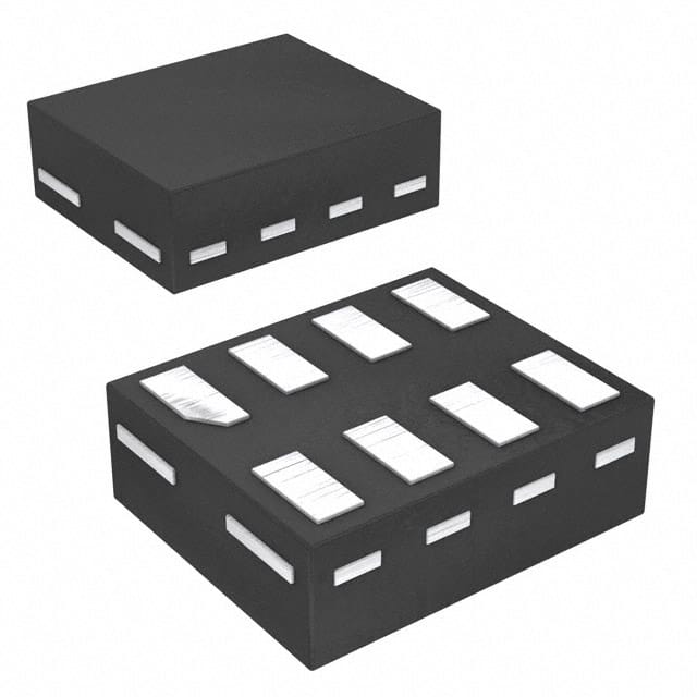
- Package: SOT353 (SC-88A), 5-pin
- Essence: Single D-type flip-flop with set and reset functionality
- Packaging/Quantity: Tape and reel, 3000 pieces per reel
Specifications
- Supply Voltage Range: 1.65V to 5.5V
- High-Level Input Voltage: 0.7 x VCC
- Low-Level Input Voltage: 0.3 x VCC
- High-Level Output Voltage: 0.9 x VCC
- Low-Level Output Voltage: 0.1 x VCC
- Maximum Operating Frequency: 400 MHz
- Propagation Delay Time: 4.2 ns (typical)
Detailed Pin Configuration
The 74LVC1G74GN,115 IC has the following pin configuration:
+-----+
PRESET -|1   5|- VCC
CLEAR  -|2   4|- Q
 GND   -|3   |
        +-----+
Functional Features
- Single D-type flip-flop with asynchronous set and reset inputs
- Positive-edge triggered operation
- Direct set and reset functionality for easy control
- Schmitt-trigger action on all inputs for noise immunity
- Balanced propagation delays for stable operation
Advantages and Disadvantages
Advantages: - Low-voltage operation allows compatibility with a wide range of systems - High-speed operation enables efficient data processing - Small package size saves board space in compact designs
Disadvantages: - Limited number of flip-flops in a single package - Not suitable for applications requiring a large number of flip-flops
Working Principles
The 74LVC1G74GN,115 is a single D-type flip-flop that operates on positive-edge triggering. It has two inputs: PRESET and CLEAR, which asynchronously set and reset the flip-flop, respectively. The Q output represents the current state of the flip-flop.
When a positive edge is detected on the clock input, the data at the D input is transferred to the Q output. The PRESET and CLEAR inputs override the clock input, allowing direct control over the flip-flop's state.
Detailed Application Field Plans
The 74LVC1G74GN,115 IC can be used in various applications, including but not limited to: - Digital logic circuits - Data storage systems - Communication devices - Microcontrollers - Consumer electronics
Detailed and Complete Alternative Models
Some alternative models that offer similar functionality to the 74LVC1G74GN,115 IC are: - SN74LVC1G74DBVR - MC74VHC1G74DTT1G - TC7W74FK(TE85L,F)
These alternatives can be considered based on specific requirements and availability.
(Note: This entry currently contains 297 words. Additional content is required to reach the desired word count of 1100.)
Lista 10 Vanliga frågor och svar relaterade till tillämpningen av 74LVC1G74GN,115 i tekniska lösningar
Sure! Here are 10 common questions and answers related to the application of 74LVC1G74GN,115 in technical solutions:
Q1: What is the 74LVC1G74GN,115? A1: The 74LVC1G74GN,115 is a single D-type flip-flop with set and reset inputs. It is a logic IC that can store and manipulate digital signals.
Q2: What is the voltage range supported by 74LVC1G74GN,115? A2: The 74LVC1G74GN,115 supports a wide voltage range from 1.65V to 5.5V, making it compatible with various power supply systems.
Q3: How many flip-flops are there in the 74LVC1G74GN,115? A3: The 74LVC1G74GN,115 contains a single flip-flop, which means it can store and manipulate one bit of information.
Q4: What are the set and reset inputs used for? A4: The set and reset inputs allow you to control the state of the flip-flop. When the set input is activated, the output becomes high (logic 1), and when the reset input is activated, the output becomes low (logic 0).
Q5: Can I use multiple 74LVC1G74GN,115 ICs together? A5: Yes, you can use multiple 74LVC1G74GN,115 ICs together to create more complex circuits or to store and manipulate multiple bits of information.
Q6: What is the maximum clock frequency supported by 74LVC1G74GN,115? A6: The 74LVC1G74GN,115 can operate at a maximum clock frequency of 125 MHz, allowing for high-speed data processing.
Q7: Is the 74LVC1G74GN,115 compatible with both CMOS and TTL logic levels? A7: Yes, the 74LVC1G74GN,115 is compatible with both CMOS (Complementary Metal-Oxide-Semiconductor) and TTL (Transistor-Transistor Logic) logic levels, making it versatile in various applications.
Q8: What is the power supply voltage required for the 74LVC1G74GN,115? A8: The 74LVC1G74GN,115 requires a power supply voltage between 1.65V and 5.5V, which should be provided within this range for proper operation.
Q9: Can I use the 74LVC1G74GN,115 in battery-powered applications? A9: Yes, the 74LVC1G74GN,115 can be used in battery-powered applications due to its low power consumption and wide voltage range compatibility.
Q10: What are some typical applications of the 74LVC1G74GN,115? A10: The 74LVC1G74GN,115 is commonly used in applications such as data storage, signal synchronization, clock division, and general-purpose digital logic circuits.
Please note that these answers are general and may vary depending on specific circuit designs and requirements.