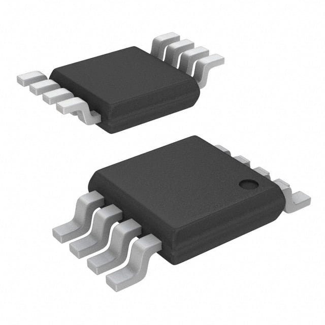
74LVC1G53DP,125
Basic Information Overview
- Category: Integrated Circuit (IC)
- Use: Logic Gate
- Characteristics: Single 2-input AND gate with Schmitt-trigger inputs
- Package: SOT353 (SC-88A)
- Essence: High-speed CMOS technology
- Packaging/Quantity: Tape and Reel, 3000 pieces per reel
Specifications
- Supply Voltage Range: 1.65V to 5.5V
- Input Voltage Range: -0.5V to VCC + 0.5V
- Output Voltage Range: GND to VCC
- Operating Temperature Range: -40°C to +125°C
- Propagation Delay: 4.3 ns at 3.3V, 6.8 ns at 1.8V
- Quiescent Current: 10 µA at 3.3V, 1 µA at 1.8V
Detailed Pin Configuration
The 74LVC1G53DP,125 has a total of 5 pins: 1. Pin 1: Input A 2. Pin 2: Input B 3. Pin 3: Ground (GND) 4. Pin 4: Output (Y) 5. Pin 5: Power Supply (VCC)
Functional Features
- Schmitt-trigger inputs for noise immunity
- High-speed operation
- Low power consumption
- Wide supply voltage range
- Compatible with TTL levels
- Balanced propagation delays
Advantages and Disadvantages
Advantages: - Provides noise immunity due to Schmitt-trigger inputs - Offers high-speed operation for time-critical applications - Low power consumption helps in energy-efficient designs - Wide supply voltage range allows compatibility with various systems - TTL level compatibility simplifies interfacing with other devices - Balanced propagation delays ensure accurate signal transmission
Disadvantages: - Limited to 2-input AND gate functionality - SOT353 package may require specialized handling during assembly
Working Principles
The 74LVC1G53DP,125 is a single 2-input AND gate with Schmitt-trigger inputs. It operates based on the principles of CMOS technology, which allows for high-speed and low-power logic operations. The Schmitt-trigger inputs provide noise immunity by ensuring that the output transitions occur at well-defined voltage levels, even in the presence of input signal fluctuations.
Detailed Application Field Plans
The 74LVC1G53DP,125 can be used in various applications, including: 1. Digital signal processing systems 2. Communication equipment 3. Industrial control systems 4. Automotive electronics 5. Battery-powered devices 6. Consumer electronics
Detailed and Complete Alternative Models
Some alternative models that offer similar functionality to the 74LVC1G53DP,125 are: 1. SN74LVC1G53DBVR - Texas Instruments 2. MC74VHC1G53DTT1G - ON Semiconductor 3. NCV8533DTRKG - ON Semiconductor 4. TC7SZ53FU(TE85L,F) - Toshiba Semiconductor
Note: This list is not exhaustive, and there may be other alternative models available from different manufacturers.
In conclusion, the 74LVC1G53DP,125 is a single 2-input AND gate IC with Schmitt-trigger inputs. It offers high-speed operation, low power consumption, and noise immunity. Its wide supply voltage range and TTL compatibility make it suitable for various applications in digital systems.
Lista 10 Vanliga frågor och svar relaterade till tillämpningen av 74LVC1G53DP,125 i tekniska lösningar
Sure! Here are 10 common questions and answers related to the application of 74LVC1G53DP,125:
Q1: What is the 74LVC1G53DP,125? A1: The 74LVC1G53DP,125 is a single multiplexer/demultiplexer IC (Integrated Circuit) with two inputs and one output.
Q2: What is the voltage range supported by the 74LVC1G53DP,125? A2: The 74LVC1G53DP,125 supports a voltage range from 1.65V to 5.5V.
Q3: How many channels does the 74LVC1G53DP,125 have? A3: The 74LVC1G53DP,125 has one channel, which means it can handle one input and one output at a time.
Q4: Can the 74LVC1G53DP,125 be used as both a multiplexer and a demultiplexer? A4: Yes, the 74LVC1G53DP,125 can be used as both a multiplexer and a demultiplexer depending on the configuration.
Q5: What is the maximum data rate supported by the 74LVC1G53DP,125? A5: The 74LVC1G53DP,125 supports a maximum data rate of 400 Mbps (megabits per second).
Q6: Does the 74LVC1G53DP,125 have any built-in protection features? A6: Yes, the 74LVC1G53DP,125 has built-in ESD (Electrostatic Discharge) protection to prevent damage from static electricity.
Q7: Can the 74LVC1G53DP,125 be used in battery-powered applications? A7: Yes, the 74LVC1G53DP,125 is suitable for battery-powered applications due to its low power consumption.
Q8: What is the package type of the 74LVC1G53DP,125? A8: The 74LVC1G53DP,125 is available in a small SOT-353 package.
Q9: Can the 74LVC1G53DP,125 handle analog signals? A9: No, the 74LVC1G53DP,125 is a digital IC and is designed to handle digital signals only.
Q10: Are there any recommended applications for the 74LVC1G53DP,125? A10: The 74LVC1G53DP,125 is commonly used in various applications such as data multiplexing, signal routing, and general-purpose switching.
Please note that these answers are based on general knowledge and may vary depending on specific use cases and datasheet specifications.


