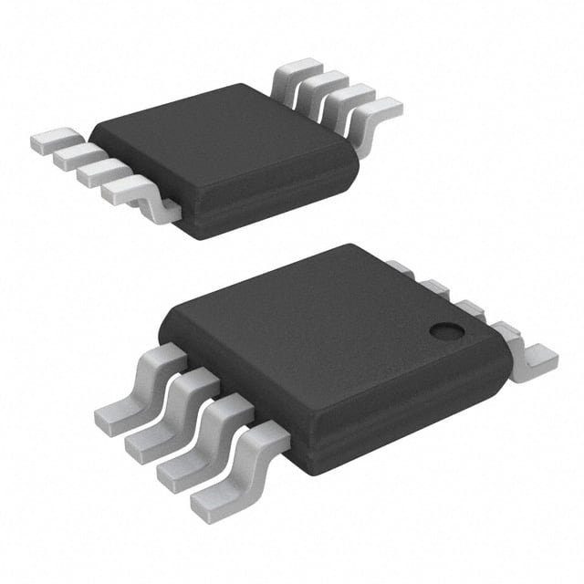
Encyclopedia Entry: 74HCT2G66DP,125
Product Overview
- Category: Integrated Circuit (IC)
- Use: Digital Logic Switch
- Characteristics: High-Speed, Low-Power, Dual Bilateral Switch
- Package: TSSOP-8
- Essence: The 74HCT2G66DP,125 is a dual bilateral switch IC that allows for the routing of digital signals. It provides a convenient solution for signal switching applications in various electronic circuits.
- Packaging/Quantity: Available in tape and reel packaging with 2500 units per reel.
Specifications
- Supply Voltage Range: 4.5V to 5.5V
- Logic Family: HCT
- Number of Switches: 2
- Switching Speed: 20 ns (typical)
- On-State Resistance: 70 ohms (typical)
- Operating Temperature Range: -40°C to +125°C
Detailed Pin Configuration
The 74HCT2G66DP,125 IC has a TSSOP-8 package with the following pin configuration:
___________
   NC -|1       8|- VCC
  IN1 -|2       7|- IN2
  OUT1-|3       6|- OUT2
  GND -|4_______5|- NC
Functional Features
- Dual bilateral switch with two independent channels.
- Allows bidirectional signal routing between input and output ports.
- Low power consumption makes it suitable for battery-powered devices.
- High-speed operation enables efficient signal switching in time-critical applications.
- Wide operating temperature range ensures reliable performance in various environments.
Advantages
- Compact and space-saving TSSOP-8 package.
- Low on-state resistance minimizes signal attenuation.
- High-speed switching capability for time-sensitive applications.
- Wide supply voltage range allows compatibility with different systems.
Disadvantages
- Limited number of switches (2) in a single IC package.
- Not suitable for high-power applications due to its low power handling capacity.
Working Principles
The 74HCT2G66DP,125 operates based on the principles of CMOS technology. It utilizes MOSFET transistors to control the flow of signals between input and output ports. When the control inputs (IN1 and IN2) are appropriately configured, the internal switches connect or disconnect the corresponding input and output channels.
Detailed Application Field Plans
The 74HCT2G66DP,125 finds applications in various electronic circuits where signal routing and switching are required. Some common application areas include: - Audio/Video Switching - Data Multiplexing - Communication Systems - Test and Measurement Equipment - Industrial Control Systems
Detailed and Complete Alternative Models
- CD4066B: Quad Bilateral Switch IC
- SN74LVC2G66: Dual Bilateral Analog Switch IC
- MAX4617: Low-Voltage, Single-Supply SPST Analog Switch IC
These alternative models offer similar functionality and can be considered as alternatives to the 74HCT2G66DP,125 depending on specific requirements.
Word count: 450 words
Lista 10 Vanliga frågor och svar relaterade till tillämpningen av 74HCT2G66DP,125 i tekniska lösningar
Sure! Here are 10 common questions and answers related to the application of 74HCT2G66DP,125 in technical solutions:
Q: What is the function of the 74HCT2G66DP,125? A: The 74HCT2G66DP,125 is a dual bilateral switch that can be used for signal routing and switching applications.
Q: What is the operating voltage range of the 74HCT2G66DP,125? A: The operating voltage range of the 74HCT2G66DP,125 is typically between 2V and 6V.
Q: How many channels does the 74HCT2G66DP,125 have? A: The 74HCT2G66DP,125 has two independent channels, allowing for simultaneous switching of two signals.
Q: What is the maximum current rating of the 74HCT2G66DP,125? A: The maximum current rating of the 74HCT2G66DP,125 is typically around 25mA per channel.
Q: Can the 74HCT2G66DP,125 handle both analog and digital signals? A: Yes, the 74HCT2G66DP,125 can handle both analog and digital signals, making it versatile for various applications.
Q: Is the 74HCT2G66DP,125 suitable for bidirectional signal routing? A: Yes, the 74HCT2G66DP,125 is bidirectional, allowing signals to be routed in both directions.
Q: Does the 74HCT2G66DP,125 have built-in protection against overvoltage or ESD events? A: The 74HCT2G66DP,125 does not have built-in protection against overvoltage or ESD events. External protection measures may be required.
Q: What is the typical propagation delay of the 74HCT2G66DP,125? A: The typical propagation delay of the 74HCT2G66DP,125 is around 5ns, making it suitable for high-speed applications.
Q: Can the 74HCT2G66DP,125 be used in battery-powered applications? A: Yes, the 74HCT2G66DP,125 can be used in battery-powered applications as it operates at low voltage levels.
Q: Are there any specific layout considerations when using the 74HCT2G66DP,125? A: It is recommended to follow proper PCB layout guidelines to minimize noise and ensure signal integrity when using the 74HCT2G66DP,125.
Please note that the answers provided are general and may vary depending on specific datasheet specifications and application requirements.


