

Encyclopedia Entry: 74HCT2G34GV,125
Product Overview
- Category: Integrated Circuit (IC)
- Use: Logic Gate
- Characteristics: High-Speed, Low-Power, Dual Inverter
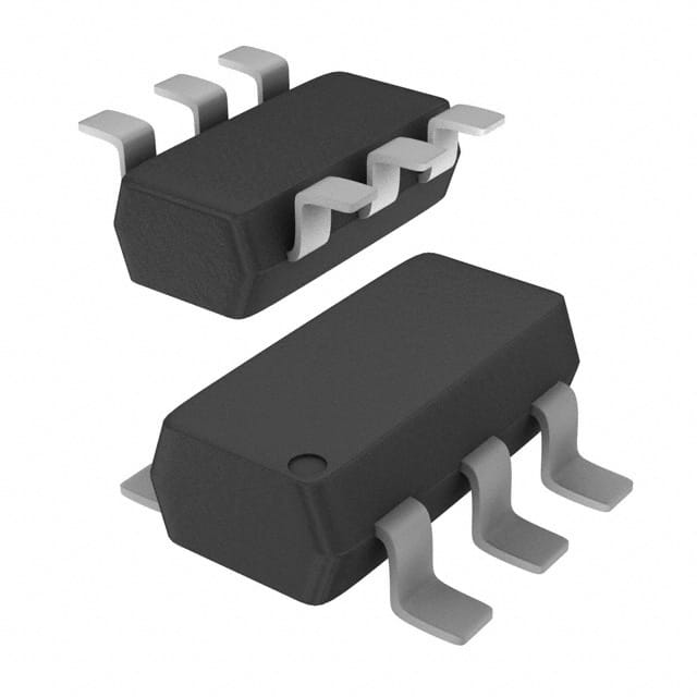
- Package: SOT353 (SC-88A)
- Essence: Transistor-Transistor Logic (TTL) Compatible Inverter
- Packaging/Quantity: Tape and Reel, 3000 units per reel
Specifications
- Supply Voltage: 2.0V to 5.5V
- Input Voltage: 0V to VCC
- Output Voltage: 0V to VCC
- Operating Temperature Range: -40°C to +125°C
- Propagation Delay: 7 ns (typical)
- Output Current: ±4 mA
- Input Capacitance: 3 pF (typical)
Detailed Pin Configuration
The 74HCT2G34GV,125 has a total of 6 pins: 1. Pin 1: Input A 2. Pin 2: Output A 3. Pin 3: GND (Ground) 4. Pin 4: Input B 5. Pin 5: Output B 6. Pin 6: VCC (Supply Voltage)
Functional Features
- Dual Inverter: The 74HCT2G34GV,125 consists of two independent inverters in a single package.
- TTL Compatibility: It is designed to be compatible with Transistor-Transistor Logic (TTL) levels, allowing seamless integration with existing TTL-based systems.
- High-Speed Operation: With a propagation delay of only 7 ns, this IC enables fast switching between logic states.
- Low Power Consumption: The 74HCT2G34GV,125 operates at a low supply voltage range of 2.0V to 5.5V, making it suitable for battery-powered devices.
Advantages and Disadvantages
Advantages: - Compact Size: The SOT353 package offers a small footprint, saving valuable board space. - Wide Operating Voltage Range: It can operate within a wide range of supply voltages, providing flexibility in various applications. - Compatibility: TTL compatibility allows easy integration with existing systems.
Disadvantages: - Limited Output Current: The output current is limited to ±4 mA, which may restrict its use in certain high-current applications. - Input Capacitance: The input capacitance of 3 pF may affect the performance in high-frequency applications.
Working Principles
The 74HCT2G34GV,125 is based on Transistor-Transistor Logic (TTL) technology. It utilizes two complementary metal-oxide-semiconductor (CMOS) inverters to perform logic inversion. When an input signal is applied, the corresponding output signal will be inverted. The IC operates by controlling the flow of current through the transistors, resulting in the desired logic function.
Detailed Application Field Plans
The 74HCT2G34GV,125 finds applications in various fields, including: 1. Digital Electronics: It is commonly used in digital circuits for logic inversion and signal buffering. 2. Microcontrollers: It can be employed as an interface between microcontrollers and other digital components. 3. Communication Systems: The IC can be utilized in communication systems for signal processing and level shifting. 4. Consumer Electronics: It is suitable for use in portable devices, such as smartphones and tablets, due to its low power consumption and compact size.
Detailed and Complete Alternative Models
Some alternative models that offer similar functionality to the 74HCT2G34GV,125 include: - SN74LVC2G34: Dual Inverter, Low-Voltage CMOS Logic - MC74VHC1G14: Single Inverter with Schmitt Trigger Input, High-Speed CMOS Logic - CD74HCT04: Hex Inverter, High-Speed CMOS Logic
These alternative models can be considered based on specific requirements and compatibility with existing systems.
In conclusion, the 74HCT2G34GV,125 is a high-speed, low-power dual inverter IC that finds applications in digital electronics, microcontrollers, communication systems, and consumer electronics. Its compact size, wide operating voltage range, and TTL compatibility make it a versatile choice for various logic inversion and signal buffering tasks.
Lista 10 Vanliga frågor och svar relaterade till tillämpningen av 74HCT2G34GV,125 i tekniska lösningar
Sure! Here are 10 common questions and answers related to the application of 74HCT2G34GV,125 in technical solutions:
Q: What is the function of the 74HCT2G34GV,125? A: The 74HCT2G34GV,125 is a dual buffer with Schmitt-trigger inputs. It is used to amplify and shape digital signals.
Q: What is the operating voltage range for the 74HCT2G34GV,125? A: The operating voltage range for this IC is typically between 4.5V and 5.5V.
Q: Can the 74HCT2G34GV,125 be used as a level shifter? A: Yes, it can be used as a level shifter to convert signals from one voltage level to another.
Q: What is the maximum output current of the 74HCT2G34GV,125? A: The maximum output current is typically around 8mA.
Q: Is the 74HCT2G34GV,125 suitable for high-speed applications? A: Yes, it has a fast propagation delay and can be used in high-speed applications.
Q: Can I use the 74HCT2G34GV,125 in both CMOS and TTL logic systems? A: Yes, it is compatible with both CMOS and TTL logic levels.
Q: Does the 74HCT2G34GV,125 have built-in protection against electrostatic discharge (ESD)? A: Yes, it has ESD protection on all pins, making it more robust against static electricity.
Q: What is the package type for the 74HCT2G34GV,125? A: It is available in a small SOT353 package.
Q: Can I use the 74HCT2G34GV,125 in battery-powered applications? A: Yes, it has low power consumption and can be used in battery-powered devices.
Q: Are there any specific application notes or reference designs available for the 74HCT2G34GV,125? A: Yes, you can refer to the datasheet provided by the manufacturer for detailed application information and example circuits.
Please note that the answers provided here are general and may vary depending on specific design requirements and conditions.