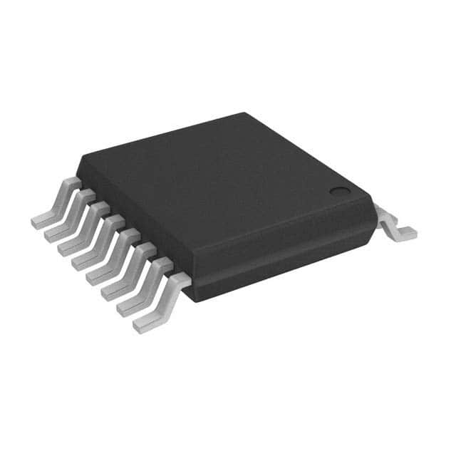
74HC4050PW,112
Basic Information Overview
- Category: Integrated Circuit (IC)
- Use: Level shifting and signal conditioning
- Characteristics: High-speed CMOS logic, low power consumption
- Package: TSSOP (Thin Shrink Small Outline Package)
- Essence: Hex non-inverting buffer/converters
- Packaging/Quantity: Tape and reel, 2500 pieces per reel
Specifications
- Supply Voltage Range: 2.0V to 6.0V
- Input Voltage Range: GND to VCC
- Output Voltage Range: GND to VCC
- Maximum Input Current: ±20mA
- Maximum Output Current: ±25mA
- Propagation Delay Time: 10ns (typical)
- Operating Temperature Range: -40°C to +125°C
Detailed Pin Configuration
The 74HC4050PW,112 IC has a total of 16 pins arranged as follows:
+-----+
   A1 -|1   16|- VCC
   A2 -|2   15|- Y1
   A3 -|3   14|- Y2
   A4 -|4   13|- Y3
   A5 -|5   12|- Y4
   A6 -|6   11|- Y5
  GND -|7   10|- Y6
   B1 -|8    9|- Y7
       +-----+
Functional Features
- Hex non-inverting buffer/converters with high noise immunity
- Wide voltage range compatibility for level shifting applications
- Can be used as line drivers, CMOS to TTL converters, or CMOS to CMOS level shifters
- Low power consumption makes it suitable for battery-powered devices
- High-speed operation allows for efficient signal conditioning
Advantages and Disadvantages
Advantages: - High noise immunity ensures reliable signal transmission - Wide voltage range compatibility enhances versatility - Low power consumption prolongs battery life - Fast propagation delay time enables quick signal processing
Disadvantages: - Limited output current may restrict certain applications - TSSOP package may require careful handling during assembly
Working Principles
The 74HC4050PW,112 is a hex non-inverting buffer/converters IC that operates on high-speed CMOS logic. It is designed to shift the voltage levels of digital signals while providing signal conditioning. The IC accepts input signals within the specified voltage range and produces corresponding output signals with improved noise immunity. By utilizing a CMOS technology, it achieves low power consumption, making it suitable for various portable and battery-powered devices.
Detailed Application Field Plans
The 74HC4050PW,112 IC finds applications in various fields such as: 1. Communication systems: Signal level shifting and conditioning in data transmission circuits. 2. Industrial automation: Interface conversion between different logic families. 3. Consumer electronics: Voltage level adaptation in audio/video equipment. 4. Automotive electronics: Signal buffering and conversion in automotive control systems. 5. Medical devices: Level shifting and signal conditioning in medical monitoring equipment.
Detailed and Complete Alternative Models
Some alternative models to the 74HC4050PW,112 IC include: - CD4050BE: DIP package, similar functionality - SN74HC4050N: DIP package, higher operating temperature range - MC14050BCL: SOIC package, wider supply voltage range
These alternative models offer similar functionality and can be used as replacements depending on specific requirements.
Word count: 346 words
Lista 10 Vanliga frågor och svar relaterade till tillämpningen av 74HC4050PW,112 i tekniska lösningar
Sure! Here are 10 common questions and answers related to the application of 74HC4050PW,112 in technical solutions:
Q: What is the function of the 74HC4050PW,112? A: The 74HC4050PW,112 is a hex non-inverting buffer with high-to-low level shifting capabilities.
Q: What voltage levels can the 74HC4050PW,112 handle? A: The 74HC4050PW,112 can handle voltage levels from 2V to 6V.
Q: Can the 74HC4050PW,112 be used for level shifting between different voltage domains? A: Yes, the 74HC4050PW,112 can be used for level shifting between different voltage domains.
Q: How many input/output pins does the 74HC4050PW,112 have? A: The 74HC4050PW,112 has six input/output pins.
Q: What is the maximum output current that the 74HC4050PW,112 can provide? A: The 74HC4050PW,112 can provide a maximum output current of 25mA.
Q: Can the 74HC4050PW,112 be used as a voltage translator? A: Yes, the 74HC4050PW,112 can be used as a voltage translator between different logic levels.
Q: Is the 74HC4050PW,112 compatible with both CMOS and TTL logic levels? A: Yes, the 74HC4050PW,112 is compatible with both CMOS and TTL logic levels.
Q: Can the 74HC4050PW,112 be used for signal buffering and line driving? A: Yes, the 74HC4050PW,112 can be used for signal buffering and line driving applications.
Q: What is the typical propagation delay of the 74HC4050PW,112? A: The typical propagation delay of the 74HC4050PW,112 is around 15ns.
Q: Can the 74HC4050PW,112 be used in high-speed digital communication systems? A: Yes, the 74HC4050PW,112 can be used in high-speed digital communication systems due to its fast switching characteristics.
Please note that the specific details and answers may vary depending on the application and context.


