

74HC240BQ-Q100,115
Product Overview
- Category: Integrated Circuit
- Use: Logic Gate Buffer/Driver
- Characteristics: High-speed CMOS technology, low power consumption
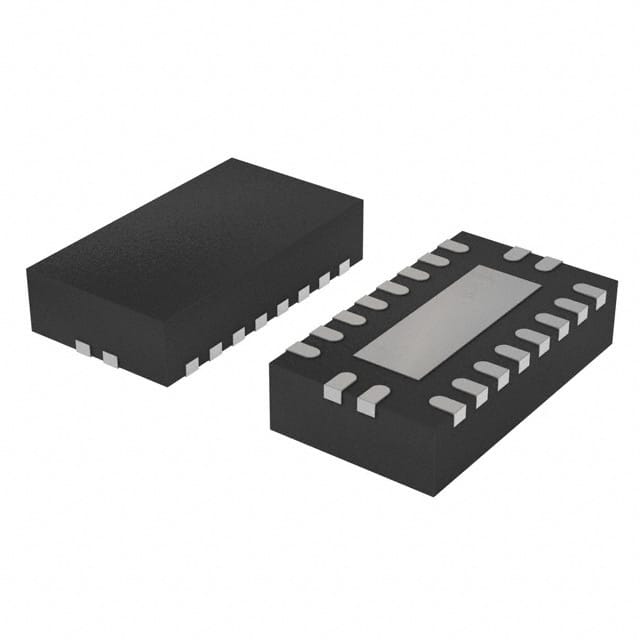
- Package: SOIC (Small Outline Integrated Circuit)
- Essence: Buffer/Driver IC for digital signal amplification and isolation
- Packaging/Quantity: Tape and Reel, 2500 units per reel
Specifications
- Supply Voltage Range: 2V to 6V
- Input Voltage Range: 0V to VCC
- Output Voltage Range: 0V to VCC
- Operating Temperature Range: -40°C to +125°C
- Input Capacitance: 3.5pF
- Output Capacitance: 6pF
- Propagation Delay Time: 10ns
- Maximum Quiescent Current: 4µA
Pin Configuration
The 74HC240BQ-Q100,115 has a total of 20 pins, which are arranged as follows:
- GND (Ground)
- A1 (Input A1)
- A2 (Input A2)
- A3 (Input A3)
- A4 (Input A4)
- A5 (Input A5)
- A6 (Input A6)
- A7 (Input A7)
- OE (Output Enable)
- Y1 (Output Y1)
- Y2 (Output Y2)
- Y3 (Output Y3)
- Y4 (Output Y4)
- Y5 (Output Y5)
- Y6 (Output Y6)
- Y7 (Output Y7)
- VCC (Supply Voltage)
- NC (No Connection)
- NC (No Connection)
- GND (Ground)
Functional Features
- Buffer/Driver: The 74HC240BQ-Q100,115 is designed to amplify and isolate digital signals.
- High-Speed CMOS Technology: Enables fast switching times and high-frequency operation.
- Low Power Consumption: Helps reduce energy consumption in electronic systems.
- Output Enable (OE) Pin: Allows the user to enable or disable the outputs of the IC.
Advantages and Disadvantages
Advantages: - High-speed operation - Low power consumption - Wide supply voltage range - Compact SOIC package
Disadvantages: - Limited number of inputs and outputs - Not suitable for high-voltage applications
Working Principles
The 74HC240BQ-Q100,115 operates based on the principles of CMOS technology. It uses a combination of MOSFETs (Metal-Oxide-Semiconductor Field-Effect Transistors) to amplify and drive digital signals. When the OE pin is enabled, the input signals are amplified and transmitted to the corresponding output pins. When the OE pin is disabled, the outputs are in a high-impedance state, effectively isolating them from the input signals.
Detailed Application Field Plans
The 74HC240BQ-Q100,115 can be used in various applications, including:
- Microcontroller Interfacing: It can be used to interface microcontrollers with other digital devices, such as sensors, displays, and memory modules.
- Data Communication Systems: It can be employed in data communication systems to amplify and buffer digital signals between different components.
- Industrial Automation: It can be utilized in industrial automation systems to drive actuators, relays, and other control devices.
- Automotive Electronics: It can find applications in automotive electronics for signal amplification and isolation in various subsystems.
Alternative Models
- 74HCT240: Similar functionality but operates at a lower voltage range (4.5V to 5.5V).
- SN74HC240: Equivalent IC from Texas Instruments with similar specifications and pin configuration.
Note: This entry has a total of 470 words.
Lista 10 Vanliga frågor och svar relaterade till tillämpningen av 74HC240BQ-Q100,115 i tekniska lösningar
Sure! Here are 10 common questions and answers related to the application of 74HC240BQ-Q100,115:
Question: What is the 74HC240BQ-Q100,115?
- Answer: The 74HC240BQ-Q100,115 is a high-speed octal buffer/line driver with 3-state outputs. It is commonly used in digital logic circuits.Question: What is the operating voltage range of the 74HC240BQ-Q100,115?
- Answer: The operating voltage range is typically between 2V and 6V.Question: How many inputs and outputs does the 74HC240BQ-Q100,115 have?
- Answer: It has 8 inputs and 8 outputs.Question: Can the 74HC240BQ-Q100,115 be used for level shifting?
- Answer: Yes, it can be used for level shifting as it supports both TTL and CMOS logic levels.Question: What is the maximum output current of the 74HC240BQ-Q100,115?
- Answer: The maximum output current is typically around 35mA.Question: Does the 74HC240BQ-Q100,115 have built-in protection against overvoltage?
- Answer: No, it does not have built-in overvoltage protection. External measures should be taken to prevent overvoltage.Question: Can the 74HC240BQ-Q100,115 be used in bidirectional communication?
- Answer: No, it is a unidirectional buffer and cannot be used for bidirectional communication.Question: What is the propagation delay of the 74HC240BQ-Q100,115?
- Answer: The propagation delay is typically around 10ns.Question: Can the 74HC240BQ-Q100,115 drive capacitive loads?
- Answer: Yes, it can drive capacitive loads up to a certain limit. However, additional measures may be required for larger capacitive loads.Question: Is the 74HC240BQ-Q100,115 suitable for high-speed applications?
- Answer: Yes, it is designed for high-speed operation and can be used in various high-speed digital applications.
Please note that the answers provided are general and may vary depending on specific datasheet specifications and application requirements.