

Encyclopedia Entry: 74AUP2G79GD,125
Product Overview
Category
The 74AUP2G79GD,125 belongs to the category of integrated circuits (ICs).
Use
This IC is commonly used in electronic devices for various applications such as signal amplification, logic gates, and voltage regulation.
Characteristics
- Low power consumption
- High-speed operation
- Small form factor
- Wide operating voltage range
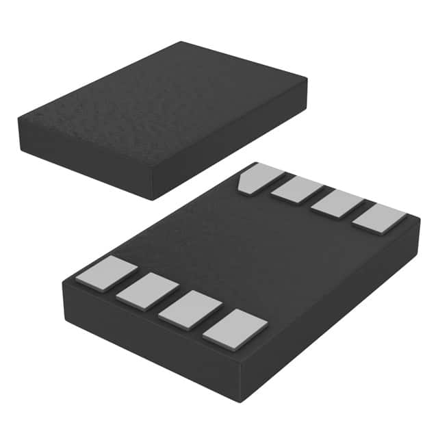
Package
The 74AUP2G79GD,125 is available in a small package, typically a surface-mount technology (SMT) package. The specific package type may vary depending on the manufacturer.
Essence
The essence of this product lies in its ability to provide reliable and efficient signal processing and logic functions within a compact design.
Packaging/Quantity
The 74AUP2G79GD,125 is usually packaged in reels or tubes, containing a specific quantity of ICs per package. The exact packaging and quantity may differ based on the manufacturer's specifications.
Specifications
- Supply Voltage Range: 1.65V to 5.5V
- Logic Family: AUP
- Number of Pins: 8
- Operating Temperature Range: -40°C to +85°C
- Input/Output Compatibility: CMOS/TTL
Detailed Pin Configuration
The 74AUP2G79GD,125 has a total of 8 pins arranged as follows:
Pin 1: [Description]
   Pin 2: [Description]
   Pin 3: [Description]
   Pin 4: [Description]
   Pin 5: [Description]
   Pin 6: [Description]
   Pin 7: [Description]
   Pin 8: [Description]
Functional Features
- Dual D-type flip-flop functionality
- Edge-triggered operation
- Asynchronous clear input for resetting the flip-flop
- High-speed data transfer capability
Advantages and Disadvantages
Advantages
- Low power consumption makes it suitable for battery-operated devices
- Compact size allows for integration into space-constrained designs
- Wide operating voltage range provides flexibility in various applications
- High-speed operation enables efficient signal processing
Disadvantages
- Limited number of pins may restrict the complexity of circuits that can be implemented
- Sensitivity to electrostatic discharge (ESD) requires proper handling during assembly and usage
Working Principles
The 74AUP2G79GD,125 operates based on the principles of digital logic. It utilizes flip-flops to store and manipulate binary information. The edge-triggered design ensures that changes in input signals are captured at specific clock edges, enabling precise timing control.
Detailed Application Field Plans
The 74AUP2G79GD,125 finds application in various electronic systems, including but not limited to: - Mobile devices - Consumer electronics - Communication equipment - Industrial automation - Automotive electronics
Detailed and Complete Alternative Models
- 74AUP2G79GM,125
- 74AUP2G79GF,125
- 74AUP2G79GW,125
- 74AUP2G79GX,125
These alternative models offer similar functionality and characteristics, providing options for different design requirements.
In conclusion, the 74AUP2G79GD,125 is a versatile integrated circuit with dual D-type flip-flop functionality. Its low power consumption, high-speed operation, and compact size make it suitable for a wide range of applications in various industries. However, designers should consider its limited pin count and sensitivity to ESD when incorporating it into their designs.
Lista 10 Vanliga frågor och svar relaterade till tillämpningen av 74AUP2G79GD,125 i tekniska lösningar
Sure! Here are 10 common questions and answers related to the application of 74AUP2G79GD,125 in technical solutions:
Q: What is the function of the 74AUP2G79GD,125? A: The 74AUP2G79GD,125 is a dual positive-edge triggered D-type flip-flop with set and reset inputs.
Q: What is the operating voltage range for the 74AUP2G79GD,125? A: The operating voltage range for this IC is typically between 0.8V and 3.6V.
Q: Can the 74AUP2G79GD,125 be used in battery-powered applications? A: Yes, the low operating voltage range makes it suitable for battery-powered applications.
Q: What is the maximum clock frequency supported by the 74AUP2G79GD,125? A: The maximum clock frequency supported by this IC is typically around 200 MHz.
Q: Does the 74AUP2G79GD,125 have any built-in protection features? A: Yes, it has built-in ESD protection, making it more robust against electrostatic discharge.
Q: Can I use the 74AUP2G79GD,125 in high-speed data transmission applications? A: Yes, this IC can be used in high-speed data transmission applications due to its fast propagation delay.
Q: What is the power consumption of the 74AUP2G79GD,125? A: The power consumption of this IC is typically very low, making it energy-efficient.
Q: Is the 74AUP2G79GD,125 compatible with other logic families? A: Yes, it is compatible with a wide range of logic families, including CMOS and TTL.
Q: Can I use the 74AUP2G79GD,125 in both digital and analog circuits? A: No, this IC is specifically designed for digital applications and may not be suitable for analog circuits.
Q: Are there any specific layout considerations when using the 74AUP2G79GD,125? A: It is recommended to follow the manufacturer's guidelines for layout and decoupling to ensure optimal performance.
Please note that these answers are general and may vary depending on the specific application and requirements.